Method for writing data in nonvolatile storage element, and nonvolatile storage device

A non-volatile storage and data writing technology, applied in the direction of information storage, static memory, digital memory information, etc., can solve problems such as difficult to achieve large capacity, achieve the effect of suppressing swing and improving retention characteristics

Inactive Publication Date: 2013-09-18
PANASONIC CORP
View PDF7 Cites 5 Cited by
  • Summary
  • Abstract
  • Description
  • Claims
  • Application Information

AI Technical Summary

Problems solved by technology

In response to such a request, there is a problem that it is difficult to increase the capacity due to the limit of the miniaturization of the conventional flash memory using a floating gate.

Method used


Image

  • Method for writing data in nonvolatile storage element, and nonvolatile storage device
  • Method for writing data in nonvolatile storage element, and nonvolatile storage device
  • Method for writing data in nonvolatile storage element, and nonvolatile storage device

Examples


Embodiment approach 1

[0058] [Structure of nonvolatile memory element]

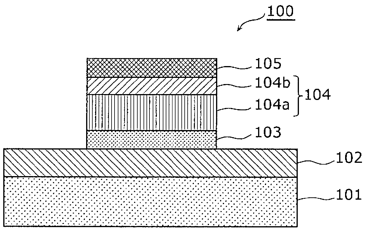
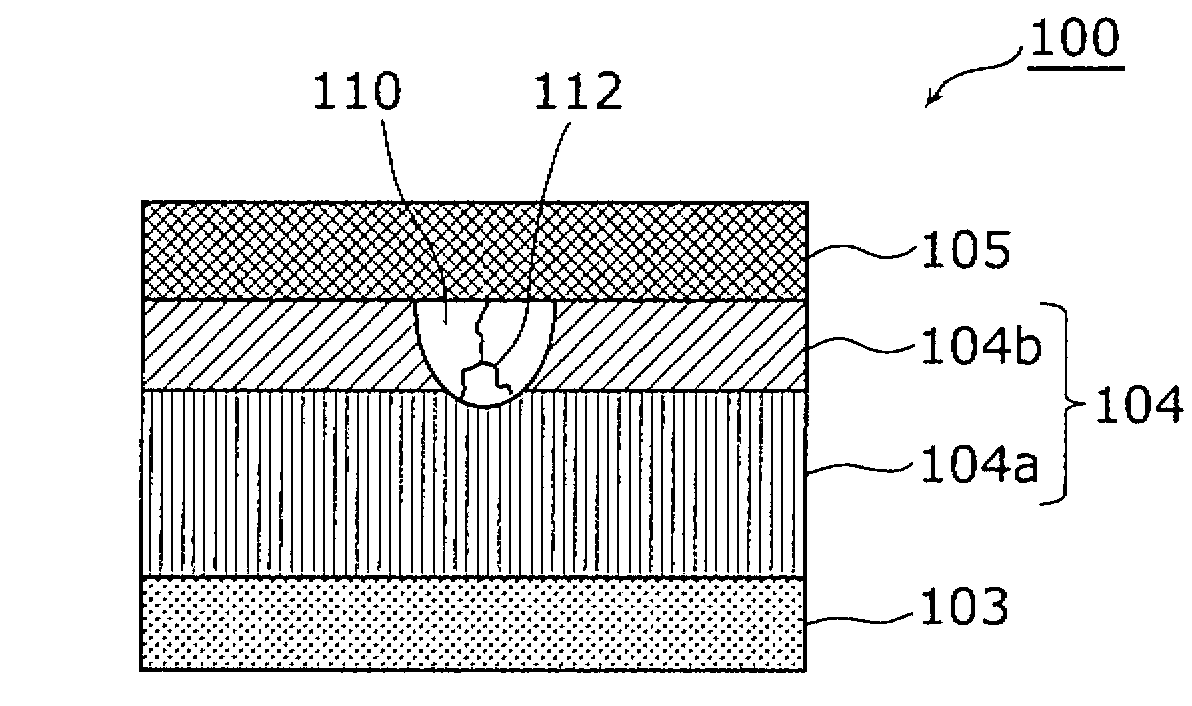
[0059] Figure 1A It is a cross-sectional view showing the structure of the nonvolatile memory element according to Embodiment 1 of the present invention.

[0060] Such as Figure 1A As shown, the nonvolatile memory element 100 of this embodiment includes a substrate 101, an interlayer insulating film 102 formed on the substrate 101, a first electrode 103 and a second electrode 105 formed on the interlayer insulating film 102. , the variable resistance layer 104 sandwiched between the first electrode 103 and the second electrode 105 . In addition, in this figure, the nonvolatile memory element 100 has the substrate 101 and the interlayer insulating film 102, but these constituent elements are not essential.

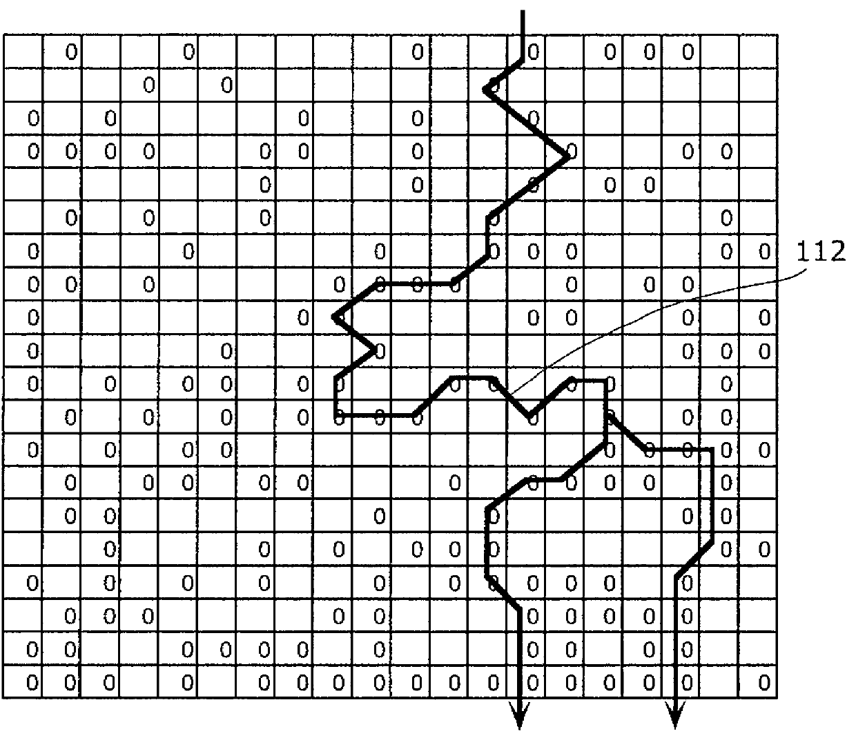
[0061] The variable resistance layer 104 has a stacked structure of a first metal oxide layer 104a including an oxide of a first metal and a second metal oxide layer 104b including an oxide of a second metal. In this em...

Embodiment approach 2

[0140] Embodiment 2 is a nonvolatile memory device of a 1-transistor / 1 nonvolatile memory unit type (so-called 1T1R type) configured using the nonvolatile memory element described in Embodiment 1. FIG.

[0141] [Structure of Nonvolatile Memory Device]

[0142] Figure 12 It is a block diagram showing an example of the configuration of the nonvolatile memory device according to Embodiment 2 of the present invention. Such as Figure 12 As shown, the nonvolatile memory device 300 of this embodiment includes: a memory cell array 301 having nonvolatile memory elements R311 to R322, an address buffer 302, a control unit 303, a row decoder 304, a word line driver 305, Column decoder 306 , bitline / plateline driver 307 . Furthermore, the bit line / plate line driver 307 has a readout circuit (sense amplifier), and can measure the current flowing through the bit line or the plate line.

[0143] The memory cell array 301 has: two word lines W1, W2 extending parallel to each other; two ...

Embodiment approach 3

[0177] Embodiment 3 is a cross-point nonvolatile memory device configured using the nonvolatile memory element described in Embodiment 1. FIG. Here, the cross-point nonvolatile memory device is a memory device of a type in which an active layer exists at an intersection point (three-dimensional intersection point) between a word line and a bit line. Next, the configuration and operation of this nonvolatile memory device will be described.

[0178] [Structure of Nonvolatile Memory Device]

[0179] Figure 13 It is a block diagram showing an example of the configuration of the nonvolatile memory device according to Embodiment 3 of the present invention. Such as Figure 13 As shown, the nonvolatile memory device 400 of this embodiment includes: a memory cell array 401 having nonvolatile memory elements R11 to R33, an address cache 402, a control unit 403, a row decoder 404, a word line driver 405, Column decoder 406, bit line driver 407. Furthermore, the bit line driver 407 ...


PUM


Abstract

Provided is a method for writing data in a nonvolatile storage element, wherein it is possible to inhibit the effects from fluctuations in resistance. The method involves: a first application step (S120) in which a first voltage pulse for changing the resistance state of a nonvolatile storage element (100) from a first state to a second state is applied; a second application step (S121) in which a second voltage pulse having the same polarity as the first voltage pulse and a smaller absolute voltage value than the first voltage pulse is applied; a determination step (S122) in which it is determined whether or not the resistance state of the nonvolatile storage element (100) is the second state; and a third application step (S123) in which a third voltage pulse for changing the resistance state of the nonvolatile storage element from the first state to the second state is applied when it is determined that the resistance state of the nonvolatile storage element (100) is not the second state.

Description

technical field [0001] The present invention relates to a data writing method of a variable resistance nonvolatile memory element whose resistance value changes according to an applied electric signal, and a nonvolatile memory device implementing the method. Background technique [0002] In recent years, electronic devices such as portable information devices and home information appliances have achieved higher functionality along with the advancement of digital technology. Therefore, there are increasing demands for increasing the capacity, reducing the writing power, shortening the writing / reading time, and extending the life of the nonvolatile memory devices mounted in these devices. In response to such a request, since there is a limit to miniaturization of the conventional flash memory using a floating gate, there is a problem that it is difficult to increase the capacity. Therefore, research and development of a nonvolatile memory device including a variable resistanc...

Claims


Application Information

Patent Timeline
Patent Type & Authority Applications(China)
IPC IPC(8): G11C13/00
CPCG11C13/0004G11C13/0064G11C13/0069G11C2013/0073G11C2013/0092G11C2213/79G11C2213/82
Inventor 高木刚魏志强
Owner PANASONIC CORP
Why Eureka
Try Eureka