High-power whole wafer flat plate pressure welding type encapsulating structure and method thereof
A technology of flat crimping and packaging structure, which is applied in the direction of electrical components, electric solid devices, circuits, etc. It can solve the problems of difficult gate crimping, affecting the balance of the mold base, and high process requirements, etc., to reduce the lead inductance , improve airtight performance, simple processing method
- Summary
- Abstract
- Description
- Claims
- Application Information
AI Technical Summary
Problems solved by technology
Method used
Image
Examples
Embodiment 1
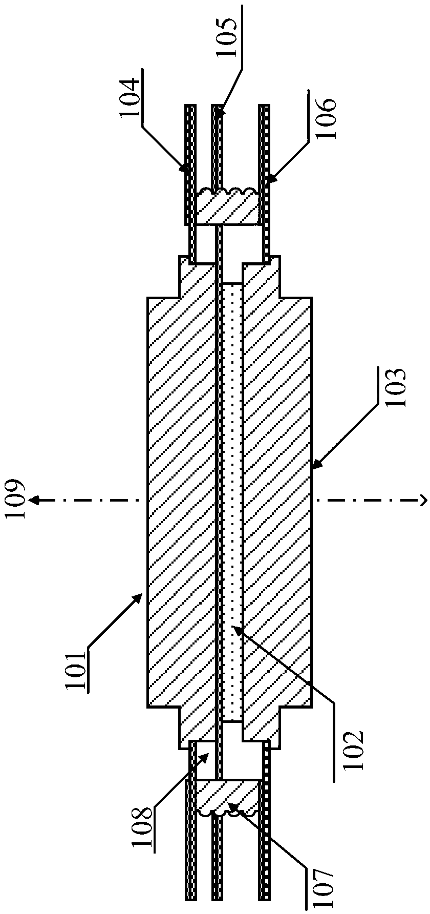
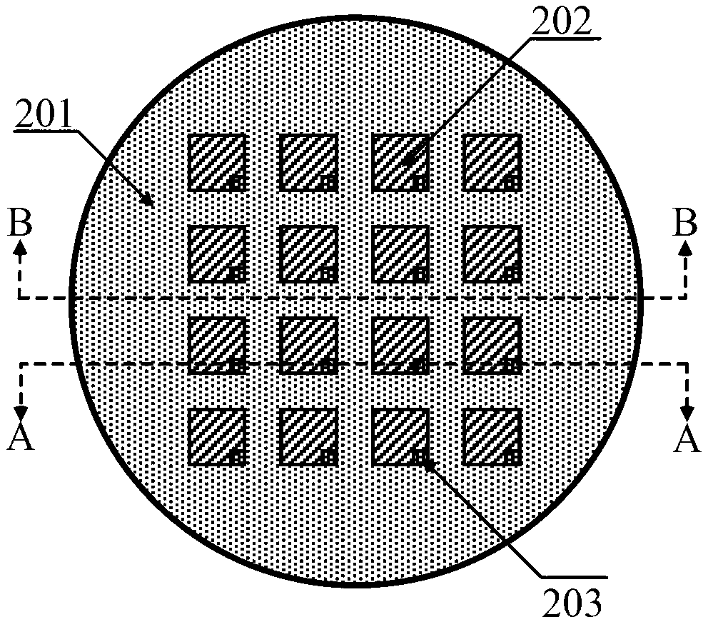
[0045] A high-power full-wafer flat crimp package structure, such as figure 1 and Figure 7 As shown, it includes an upper cover 101 and a lower cover 103 formed by crimping, and a ceramic ring 107 and a sealing assembly are arranged at both ends of the upper cover 101 and a lower cover 103. The cavity formed by the upper cover 101 and the lower cover 103 is sequentially crimped and provided with a cathode electrode Metal plate 501 , insulating layer plate 401 , gate electrode metal plate 301 , IGBT full wafer 201 and anode electrode metal plate 601 . A plurality of wafer units are distributed on the IGBT whole wafer 201, such as figure 2 As shown, the number of wafer units is 4×4, which are evenly distributed in the entire IGBT wafer 201 . The wafer unit includes an IGBT wafer cathode region 202 and an IGBT wafer gate region 203 . Cathode bump electrodes 502 are distributed on the cathode electrode metal plate 501, such as Figure 5 shown. The gate electrode metal plate...
Embodiment 2
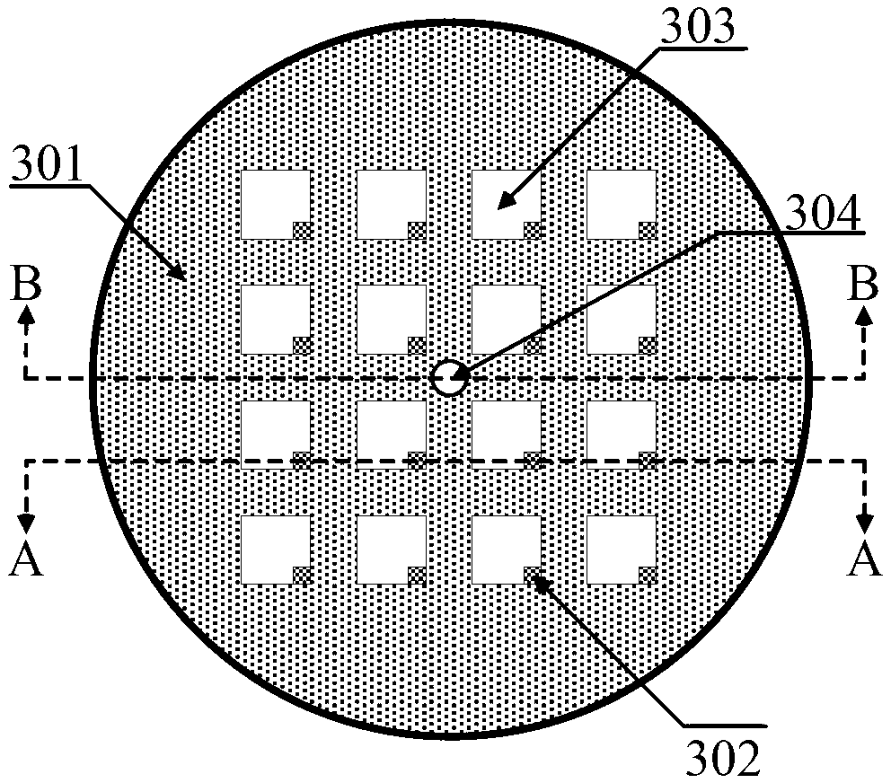
[0048] A kind of high-power full-wafer flat crimping packaging structure described in this embodiment, such as Figure 1-7 As shown, the crimping structure of the chip part includes a shell (upper cover 101 and lower cover 103) and a die 102 inside the shell (that is, an element inside the shell), wherein the upper cover 101 The cathode electrode metal plate 501, the insulating layer plate 401, the gate electrode metal plate 301 and the IGBT whole wafer 201 are sequentially crimped, the anode electrode metal plate 601 is arranged in the lower cover, the upper cover 101 and the lower cover 103 are pressed connected. A plurality of wafer units are distributed on the entire IGBT wafer 201 , and the wafer units include an IGBT wafer cathode region 202 and an IGBT wafer gate region 203 . A cathode bump electrode 502 is distributed on the cathode electrode metal plate 501, and a gate electrode bump electrode 302 and a cathode through hole 303 suitable for the cathode bump electrode...
Embodiment 3
[0060] On the basis of the above-mentioned embodiment 1 or embodiment 2, the outer surfaces of the upper cover 101 and the lower cover 103 are respectively connected to radiators, and the radiators are pressed and tightly attached to the upper cover 101 and the lower cover 103 , good cooling effect.
PUM
 Abstract
Description
Claims
Application Information
 - R&D
- Intellectual Property
- Life Sciences
- Materials
- Tech Scout
- Unparalleled Data Quality
- Higher Quality Content
- 60% Fewer Hallucinations
Browse by: Latest US Patents, China's latest patents, Technical Efficacy Thesaurus, Application Domain, Technology Topic, Popular Technical Reports.
© 2025 PatSnap. All rights reserved.Legal|Privacy policy|Modern Slavery Act Transparency Statement|Sitemap|About US| Contact US: help@patsnap.com


