High-power whole wafer flat plate pressure welding type encapsulating structure and method thereof

A flat-panel crimping, packaging structure technology, applied in electrical components, electrical solid devices, circuits, etc., can solve the problems of difficult gate crimping, high process requirements, affecting the balance of the mold frame, etc. Inductance, simple processing method, and the effect of improving airtight performance

Active Publication Date: 2015-07-08
SUZHOU YINGNENG ELECTRONICS TECH
View PDF8 Cites 0 Cited by
  • Summary
  • Abstract
  • Description
  • Claims
  • Application Information

AI Technical Summary

Problems solved by technology

[0005] In this technical solution, a high-power whole-wafer IGBT packaging structure is provided, using transition electrodes, through the positioning pins in the reserved holes of the gate pins and the missing chip positioning holes, and using the elastic gate pin unit To form the gate contact of the IGBT, and the gate pin unit includes a plastic mold base and an elastic gate pin. The gate is 4 as a unit, and a gate elastic gate pin holder is used for crimping, which can See the way using plastic formwork requires extra tedious workmanship
[0006] In the production process of the whole wafer, no matter how high the pass rate of the products on the production line is, the occurrence of failed devices cannot be avoided, that is to say, there will be bad chips at random positions throughout the whole wafer. In this technical solution In the case of bad chips, it is necessary to additionally process the gate electrodes of the bad chips on the plastic mold base, but it will inevitably affect the balance of the entire mold base, and it is difficult to ensure that the remaining good gate electrodes can be crimped well.
[0007] In addition, the distribution of the chip units in the whole IGBT wafer in this scheme is distributed in a way that the gates are close to each other in groups of 4, which is not suitable for the traditional IGBT tape-out production, and has high requirements on the process and is difficult to realize.

Method used


Image

  • High-power whole wafer flat plate pressure welding type encapsulating structure and method thereof
  • High-power whole wafer flat plate pressure welding type encapsulating structure and method thereof
  • High-power whole wafer flat plate pressure welding type encapsulating structure and method thereof

Examples


Embodiment 1

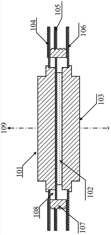
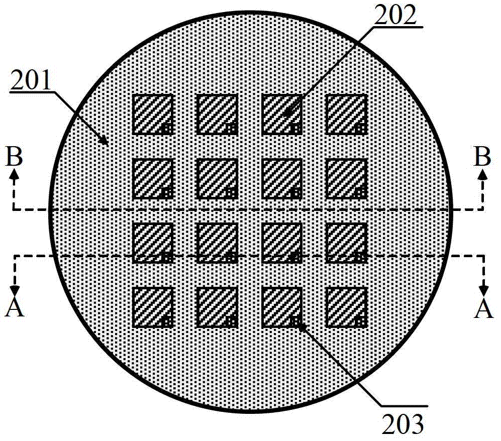
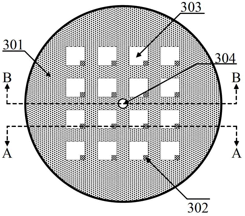
[0045] A high-power full-wafer flat crimp package structure, such as figure 1 and Figure 7 As shown, it includes an upper cover 101 and a lower cover 103 formed by crimping, and a ceramic ring 107 and a sealing assembly are arranged at both ends of the upper cover 101 and a lower cover 103. The cavity formed by the upper cover 101 and the lower cover 103 is sequentially crimped and provided with a cathode electrode Metal plate 501 , insulating layer plate 401 , gate electrode metal plate 301 , IGBT full wafer 201 and anode electrode metal plate 601 . A plurality of wafer units are distributed on the IGBT whole wafer 201, such as figure 2 As shown, the number of wafer units is 4×4, which are evenly distributed in the entire IGBT wafer 201 . The wafer unit includes an IGBT wafer cathode region 202 and an IGBT wafer gate region 203 . Cathode bump electrodes 502 are distributed on the cathode electrode metal plate 501, such as Figure 5 shown. The gate electrode metal plate...

Embodiment 2

[0048] A kind of high-power full-wafer flat crimping packaging structure described in this embodiment, such as Figure 1-7 As shown, the crimping structure of the chip part includes a shell (upper cover 101 and lower cover 103) and a die 102 inside the shell (that is, an element inside the shell), wherein the upper cover 101 The cathode electrode metal plate 501, the insulating layer plate 401, the gate electrode metal plate 301 and the IGBT whole wafer 201 are sequentially crimped, the anode electrode metal plate 601 is arranged in the lower cover, the upper cover 101 and the lower cover 103 are pressed connected. A plurality of wafer units are distributed on the entire IGBT wafer 201 , and the wafer units include an IGBT wafer cathode region 202 and an IGBT wafer gate region 203 . A cathode bump electrode 502 is distributed on the cathode electrode metal plate 501, and a gate electrode bump electrode 302 and a cathode through hole 303 suitable for the cathode bump electrode...

Embodiment 3

[0060] On the basis of the above-mentioned embodiment 1 or embodiment 2, the outer surfaces of the upper cover 101 and the lower cover 103 are respectively connected to radiators, and the radiators are pressed and tightly attached to the upper cover 101 and the lower cover 103 , good cooling effect.


PUM


Abstract

A high-power whole wafer flat plate pressure welding type encapsulating structure is formed by an upper cover and a lower cover in a pressure welding mode. A cathode electrode metal plate, an insulating layer plate, a gate pole electrode metal plate, an IGBT whole wafer and an anode electrode metal plate are sequentially arranged inside a cavity in a pressure welding mode, wherein the cavity is formed by the upper cover and the lower cover. Cathode protruding electrodes are arranged on the cathode electrode metal plate and gate pole protruding electrodes are arranged on the gate pole electrode metal plate. When a bad piece appears in one wafer unit of the whole wafer, the gate pole protruding electrode and the cathode protruding electrode which are arranged on the gate pole electrode metal plate and the cathode electrode metal plate respectively and correspond to the position of the bad piece are removed, and therefore the bad piece is prevented from being connected with the cathode electrode metal plate or the gate pole electrode metal plate. The high-power whole wafer flat plate pressure welding type encapsulating structure effectively lowers lead inductance, the reliability of a whole device is enhanced, and air impermeability performance is improved.

Description

technical field [0001] The invention relates to an IGBT packaging structure, in particular to a high-power full-wafer flat-plate crimping packaging structure and a method thereof. Background technique [0002] In the middle of the 20th century, power electronic technology developed rapidly, and power electronic devices were widely used in frequency converters. During the first world energy crisis in the early 1970s, developed countries realized energy-saving effects by using frequency conversion speed regulation. In the current environment of global energy shortage, power electronics technology, as a green energy-saving technology, plays a very important role in mechatronics, reducing environmental pollution, saving raw materials, reducing production costs and improving efficiency and quality. In the 21st century, due to the requirements of the environment, energy, society and high efficiency, power electronics is developing in the direction of high-frequency application tec...

Claims


Application Information

Patent Timeline
Patent Type & Authority Patents(China)
IPC IPC(8): H01L23/48H01L23/16H01L23/31H01L23/34H01L21/60H01L21/56
Inventor 盛况汤岑谢刚郭清
Owner SUZHOU YINGNENG ELECTRONICS TECH
Why Eureka
Try Eureka