Method for restraining warping of asymmetric printed circuit board

A printed circuit board and warpage suppression technology, which is applied in the fields of printed circuit manufacturing, printed circuit, electrical components, etc., can solve the problems of reducing production efficiency, circuit board warping rebound, increasing production cycle, etc., and achieves the improvement of production pass rate , Inhibit warpage, reduce production cost and production cycle

Active Publication Date: 2013-09-25
GUANGZHOU FASTPRINT CIRCUIT TECH
View PDF2 Cites 7 Cited by
  • Summary
  • Abstract
  • Description
  • Claims
  • Application Information

AI Technical Summary

Problems solved by technology

In order to meet special performance requirements, more and more printed circuit boards are designed with asymmetric core board thickness. Asymmetrical core board thickness will lead to asymmetrical stress during processing such as lamination, solder mask and hot air leveling. As a result, the circuit board is warped, and in severe cases, it will cause poor placement of components
At present, the main methods to solve the warping of circuit boards are: 1. Extend the lamination cooling time and release the residual stress. Using this method will cause the production cycle to double and reduce the production efficiency; 2. Pressurize after drilling Baking treatment to release mechanical pressure; 3. Hot pressing and leveling before shipment
Using the above methods increases the production cycle, reduces production efficiency, and increases additional production costs, and cannot solve the warpage problem from the source, and the circuit board will also warp and rebound, resulting in a low production pass rate

Method used


Image

  • Method for restraining warping of asymmetric printed circuit board
  • Method for restraining warping of asymmetric printed circuit board
  • Method for restraining warping of asymmetric printed circuit board

Examples


Embodiment 1

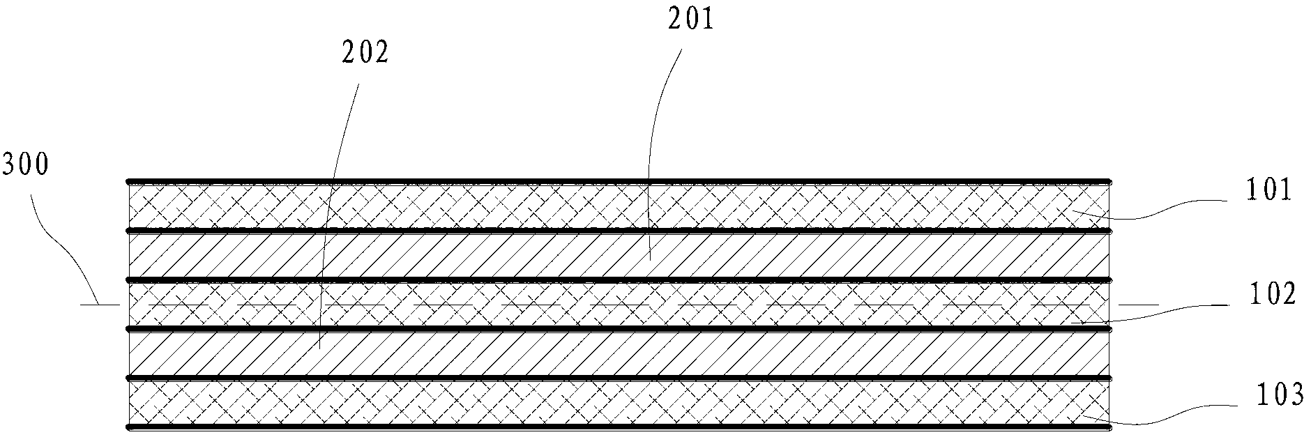
[0055] Such as image 3 As shown, this embodiment takes a six-layer printed circuit board as the design object. In this embodiment, the thickness H of the first layer core board 201 1 =0.546mm, the thickness H of the second core board 202 2 =0.136mm, the residual copper rate of each layer is between 40% and 50%, and the total plate thickness is required to be controlled at 1.4mm±10%.

[0056] Since the two layers on the outside of the printed circuit board are prepreg 100, so or due to H 1 >H 2 , and the first-layer core board 201 and the second-layer core board 202 serve as the core boards at corresponding positions on both sides of the symmetrical mirror surface 300 , so choose In this formula i=1, n=6, so Thanks to K H >1.6, so K h The value range of is [2.5,4]. In the printed circuit board of this embodiment, the first layer of prepreg 101 and the third layer of prepreg 103 are used as the prepreg 100 at the corresponding positions on both sides of the symmetri...

Embodiment 2

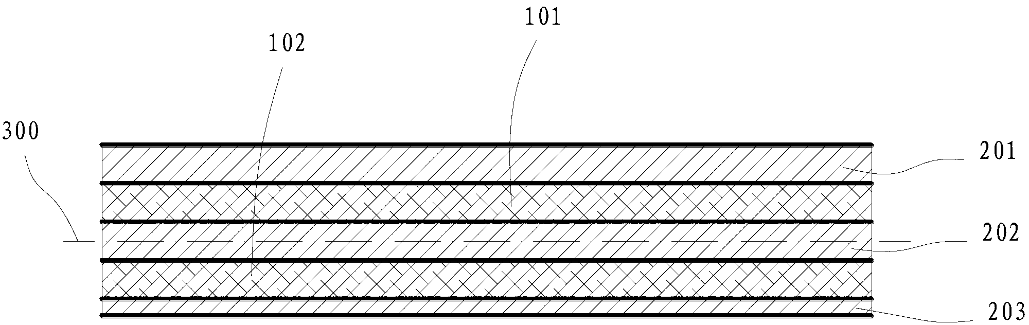
[0058] Such as Figure 4 As shown, this embodiment takes a six-layer printed circuit board as the design object. In this embodiment, the thickness H of the first layer core board 201 1 =0.746mm, the thickness H of the third core board 203 2 =0.136mm, the residual copper ratio of each layer is about 50%, and the total board thickness is required to be controlled at 2.2mm±10%.

[0059] Since the two layers on the outside of the printed circuit board are the core board 200, so or due to H 1 >H 3 , and the first-layer core board 201 and the third-layer core board 203 serve as the core boards at corresponding positions on both sides of the symmetrical mirror surface 300 , so choose In this formula i=1, n=6, so Thanks to K H >1.6, so K h The value range of is [2.5,4]. In the printed circuit board of this embodiment, the first layer of prepreg 101 and the second layer of prepreg 102 are used as prepregs at corresponding positions on both sides of the symmetrical mirror su...


PUM

PropertyMeasurementUnit
thicknessaaaaaaaaaa
thicknessaaaaaaaaaa

Abstract

The invention discloses a method for restraining warping of an asymmetric printed circuit board. According to the method for restraining the warping of the asymmetric printed circuit board, when the thicknesses of two core boards which are arranged on the corresponding positions of the two sides of a symmetrical mirror plane of the multi-layer printed circuit board are not equal, two prepregs with different thicknesses are arranged on the corresponding positions of the two sides of the symmetric mirror plane. When the thicknesses of the two core boards which are arranged on the corresponding positions of the two sides of the symmetrical mirror plane of the multi-layer printed circuit board are not equal, different kinds of thermal expansion will be generated, stress generated on one side of the symmetrical mirror plane and stress generated on the other side of the symmetrical mirror plane in the process of lamination and shrinking of resin are not equal, and therefore the warping of the printed circuit board is caused. The two prepregs with different thicknesses are arranged on the corresponding positions of the symmetric mirror plane, the prepregs generate stress, the direction of the stress generated by the prepregs is opposite to the direction of the warping of the core board, and therefore the stress generated by the core boards is counteracted. Therefore, the effect of restraining the warping is achieved, the production qualified rate of the printed circuit board is improved, the production cost is reduced, and the production cycle is shortened.

Description

technical field [0001] The invention relates to the field of printed circuit boards, in particular to a method for suppressing warpage of an asymmetric printed circuit board. Background technique [0002] The printed circuit board is an important electronic component, a support for electronic components, and a provider of electrical connections for electronic components. In order to meet special performance requirements, more and more printed circuit boards are designed with asymmetric core board thickness. Asymmetrical core board thickness will lead to asymmetrical stress during processing such as lamination, solder mask and hot air leveling. As a result, the circuit board is warped, and in severe cases, it will cause poor placement of components. At present, the main methods to solve the warping of circuit boards are: 1. Extend the lamination cooling time and release the residual stress. Using this method will cause the production cycle to double and reduce the production...

Claims


Application Information

Patent Timeline
Patent Type & Authority Applications(China)
IPC IPC(8): H05K3/00B32B5/14
Inventor 李艳国曾志军史宏宇
Owner GUANGZHOU FASTPRINT CIRCUIT TECH
Why Eureka
Try Eureka