Test path selection method and corresponding wafer test method

A test path and wafer test technology, applied in the direction of semiconductor/solid-state device test/measurement, single semiconductor device test, etc., to achieve the effect of shortening the moving distance of the probe, shortening the test time, and shortening the test path

Active Publication Date: 2016-01-20
HANGZHOU SILAN MICROELECTRONICS
View PDF10 Cites 2 Cited by
  • Summary
  • Abstract
  • Description
  • Claims
  • Application Information

AI Technical Summary

Problems solved by technology

It can be seen that the test path of this progressive scan mode is not the optimal test path

Method used


Image

  • Test path selection method and corresponding wafer test method
  • Test path selection method and corresponding wafer test method
  • Test path selection method and corresponding wafer test method

Examples


Embodiment 1

[0050] by Figure 7 shown in the flowchart as an example, combined with Figure 8 to Figure 11 , the test path selection method of the present invention will be described in detail. The test path selection method shown includes the following steps:

[0051] In step 1, a wafer is provided, the wafer being formed with dies, the dies comprising active dies and inactive dies.

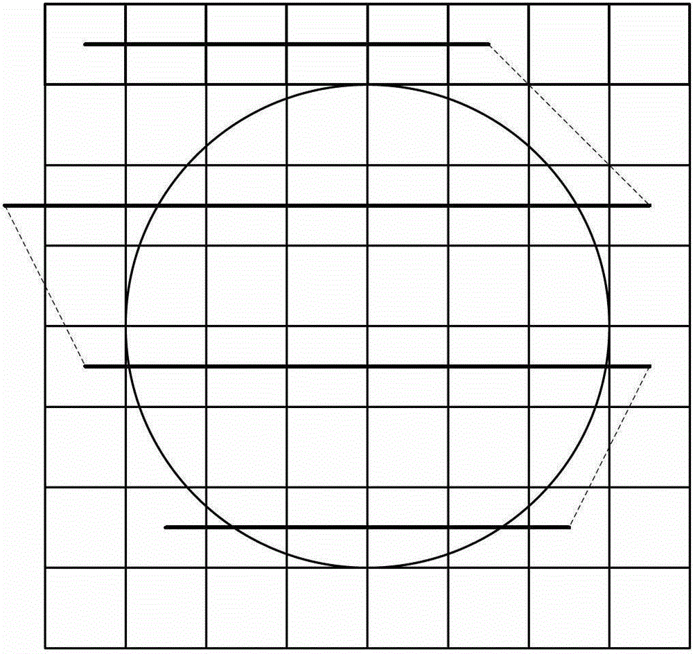
[0052] In step 2, see Figure 8 , draw and form a wafer map according to the actual size of the wafer and the size and position of the die. The wafer map is divided into a plurality of squares, each of which represents a die. The position and size of each grid on the wafer map corresponds to the position and size of the dies of the wafer one-to-one, thus forming a wafer map corresponding to the dies of the wafer one-to-one.

[0053] In step 3, see Figure 8 , using a probe to identify the positions of valid dies and invalid dies of the wafer, the squares on the wafer map are marked with different patt...

Embodiment 2

[0060] by Figure 7 shown in the flowchart as an example, combined with Figure 12 to Figure 14 , the test path selection method of the present invention will be described in detail. The test path selection method shown includes the following steps:

[0061] For Step 1 to Step 3, please refer to Step 1 to Step 3 in Embodiment 1, and details will not be repeated here.

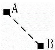
[0062] In step 4, a multi-circuit-block pin-card diagram is provided, and when the multi-circuit-block pin-card diagram is a pin-card diagram with three circuit blocks, that is, the multi-circuit-block pin-card diagram has the first pin-card mark, the second needle card mark and the third needle card mark, the straight path between the first needle card mark, the second needle card mark and the third needle card mark also forms a 0-180 degree angle with the horizontal direction angles, such as 90 degrees (see image 3 ).

[0063] According to the arrangement of the shapes and positions of the multi-circuit ...

Embodiment 3

[0068] by Figure 7 shown in the flowchart as an example, combined with Figure 15 to Figure 17 , the test path selection method of the present invention will be described in detail. The test path selection method shown includes the following steps:

[0069] For Step 1 to Step 3, please refer to Step 1 to Step 3 in Embodiment 1, and details will not be repeated here.

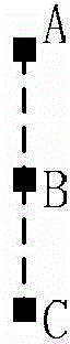
[0070] In step 4, a multi-circuit-block pin-card diagram is provided, and when the multi-circuit-block pin-card diagram is a pin-card diagram with 4 circuit blocks, that is, the multi-circuit-block pin-card diagram has the first pin-card mark, the second needle card mark, the third needle card mark and the fourth needle card mark, the straight path between the first needle card mark, the second needle card mark, the third needle card mark and the fourth needle card mark Also arranged at an angle of 0-180 degrees to the horizontal (see Figure 5 ), the angle is 45 degrees as an example for illustration.

[0...


PUM


Abstract

The invention provides a test path selection method which includes the first step of forming valid dies and invalid dies on an arranged wafer, the second step of forming a wafer mapping picture, the third step of marking the positions of the valid dies and the invalid dies on the wafer mapping picture according to the positions of the valid dies and the invalid dies, the fourth step of enabling multi-circuit-block needle card pictures to be arranged repeatedly on the dies of the wafer mapping picture and filling the wafer mapping picture, wherein the multi-circuit-block needle card pictures at least comprise a first needle card identification mark and a second needle card identification mark, the fifth step of eliminating the multi-circuit-block needle card pictures fully occupying the invalid dies on the wafer mapping picture and reserving the multi-circuit-block needle card pictures at least occupying one valid die, and the sixth step of enabling the dies corresponding to the first identification marks in each multi-circuit-block needle card picture reserved on the wafer mapping picture to be connected into a straight line, and obtaining a test path. The invention further provides a wafer test method. The test path selection method and the corresponding wafer test method shorten the distance of needle card displacement in the testing process, save needle card displacement time, and improve testing efficiency of wafers.

Description

technical field [0001] The invention belongs to the technical field of semiconductor testing, and in particular relates to a testing path selection method and a corresponding wafer testing method. Background technique [0002] After the circuits are manufactured on the wafer by semiconductor integration technology, it is necessary to test the wafer in which the circuits are manufactured before the wafer is diced. This kind of test generally tests the circuit blocks in the wafer one by one by moving the probe (Probe) on the surface of the wafer. [0003] In the existing technology, the general testing process is as follows: the wafer with the circuit manufactured is placed on the probe station, and the probe station has probes and sensors, and the probe probes the wafer through the sensor to obtain the size of the wafer. And the position of the wafer around the probe station, combined with the progressive scanning method to test the circuit blocks (ie dies) in the wafer: ...

Claims


Application Information

Patent Timeline
Patent Type & Authority Patents(China)
IPC IPC(8): G01R31/26H01L21/66
Inventor 蒋登峰
Owner HANGZHOU SILAN MICROELECTRONICS
Why Eureka
Try Eureka