Flexible copper indium gallium selenium thin film solar cell module and preparation method thereof
A thin-film solar cell, copper indium gallium selenide technology, which is applied in the field of solar cells, can solve the problems of mechanical cutter head falling into the interior of flexible substrate, difficult for laser to pass through, and short circuit of battery, so as to achieve uniform groove width, reduce damage, and improve The effect of production efficiency
- Summary
- Abstract
- Description
- Claims
- Application Information
AI Technical Summary
Problems solved by technology
Method used
Image
Examples
Embodiment 1
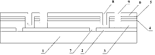
[0025] A flexible copper indium gallium selenide thin film solar cell module, such as figure 1 As shown, it consists of polyimide flexible substrate 1, double-layer Mo metal back electrode 2, copper indium gallium selenide thin film absorber layer 3, CdS buffer layer 4, intrinsic ZnO thin film barrier layer 5 and transparent conductive aluminum-doped ZnO thin film window layer 6 components and sequentially form a laminated structure, the thickness of each layer is: polyimide flexible substrate is 25 μm, the thickness of the first layer of Mo film in the double-layer Mo metal back electrode is 300nm, the thickness of the second layer of Mo film is 600nm, copper Indium gallium selenium thin film absorption layer 2μm, CdS buffer layer 60nm, intrinsic ZnO thin film barrier layer 80nm, transparent conductive aluminum-doped ZnO thin film window layer 500nm.
[0026] The preparation method of the flexible copper indium gallium selenide thin film solar cell module, the steps are as fo...
Embodiment 2
[0034] A flexible copper indium gallium selenide thin film solar cell module, such as figure 1 As shown, it is composed of stainless steel foil flexible substrate 1, double-layer Mo metal back electrode 2, copper indium gallium selenide thin film absorber layer 3, CdS buffer layer 4, intrinsic ZnO thin film barrier layer 5 and transparent conductive aluminum-doped ZnO thin film window layer 6 And sequentially form a laminated structure, the thickness of each layer is: the thickness of the stainless steel foil flexible substrate is 100 μm, the thickness of the first Mo film in the double-layer Mo metal back electrode is 100 nm, the thickness of the second Mo film is 900 nm, copper indium gallium selenide Thin-film absorption layer 1.5 μm, CdS buffer layer 80nm, intrinsic ZnO thin-film barrier layer 60nm, transparent conductive aluminum-doped ZnO thin-film window layer 350nm.
[0035] The preparation method of the flexible copper indium gallium selenide thin film solar cell modu...
PUM
| Property | Measurement | Unit |
|---|---|---|
| Thickness | aaaaa | aaaaa |
| Width | aaaaa | aaaaa |
| Thickness | aaaaa | aaaaa |
Abstract
Description
Claims
Application Information
 - R&D Engineer
- R&D Manager
- IP Professional
- Industry Leading Data Capabilities
- Powerful AI technology
- Patent DNA Extraction
Browse by: Latest US Patents, China's latest patents, Technical Efficacy Thesaurus, Application Domain, Technology Topic, Popular Technical Reports.
© 2024 PatSnap. All rights reserved.Legal|Privacy policy|Modern Slavery Act Transparency Statement|Sitemap|About US| Contact US: help@patsnap.com


