Pyroelectric thin film infrared focal plane detector chip and manufacturing method thereof

A detector chip, infrared focal plane technology, applied in the field of infrared detection, can solve the problems of difficult operation and control, increased thermal conductivity of aerogel, and high surface roughness, so as to improve stability and reliability, reduce heat Conductivity, the effect of improving sensitivity

Active Publication Date: 2015-09-09
SUZHOU INST OF NANO TECH & NANO BIONICS CHINESE ACEDEMY OF SCI +1
View PDF3 Cites 0 Cited by
  • Summary
  • Abstract
  • Description
  • Claims
  • Application Information

AI Technical Summary

Problems solved by technology

However, the preparation of this structure relies on techniques such as micromachining and sacrificial layers, and there are problems such as complex process, mismatch of thermal expansion coefficients between multilayer films in the device structure, resulting in broken electrode leads, resulting in low yield and high cost.
[0005] Especially SiO prepared by sol-gel method 2 The preparation method of airgel porous film as a thermal insulation layer requires complex and harsh process conditions, requires solvent volatilization and drying under supercritical conditions, and is affected by factors such as catalysts and side reactions of gelation reactions, so it is not suitable for controlling the formation of pore structures , affecting SiO 2 Mechanical properties and thermal conductivity reliability of airgel
This preparation method simply uses SiO 2 Airgel has obvious absorption in the 3-8μm band, which will cause SiO 2 Increased thermal conductivity of airgel
Moreover, in the process of manufacturing pyroelectric thin film infrared focal plane detector chips, repeated high-temperature annealing treatments are required, resulting in pure SiO 2 As the number of annealing increases, the porosity of airgel becomes lower and lower, and the ideal thermal insulation effect cannot be achieved, resulting in a decrease in detector sensitivity
Although in SiO 2 Airgel doped with TiO 2 Or carbon black and other infrared blocking agents, can significantly improve SiO 2 The thermal insulation efficiency of airgel at high temperature, but the doping method and process also have various difficulties, and it is difficult to operate and control
In addition, the high porosity of SiO 2 When aerogel is used as a thermal insulation structure, the surface roughness is too high, which may easily cause the detector to break down due to local high current
[0006] In summary, due to the above-mentioned limitations in the preparation process and technology, the preparation of the thermal insulation layer has become a key technical bottleneck in the production process of the pyroelectric thin film infrared focal plane detector chip

Method used


Image

  • Pyroelectric thin film infrared focal plane detector chip and manufacturing method thereof
  • Pyroelectric thin film infrared focal plane detector chip and manufacturing method thereof
  • Pyroelectric thin film infrared focal plane detector chip and manufacturing method thereof

Examples


Embodiment 1

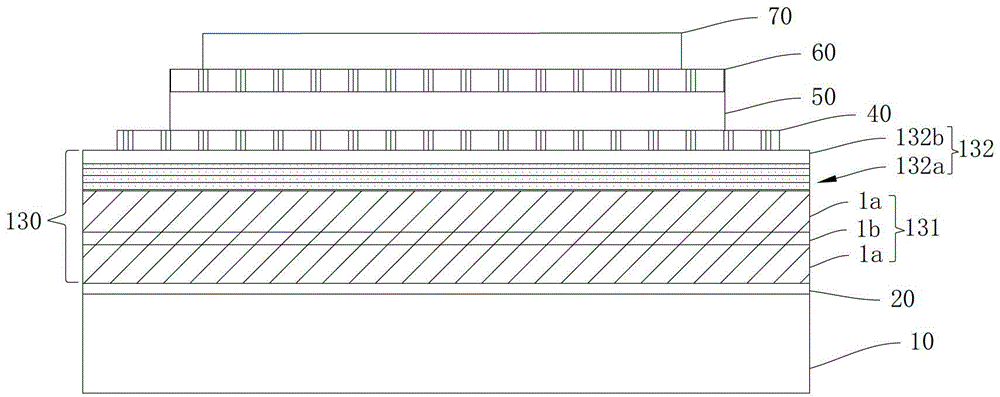
[0063] like figure 1 As shown, the pyroelectric thin film infrared focal plane detector chip of this embodiment includes, from bottom to top, a substrate 10, an adhesive layer 20, a thermally insulating support structure 130, a lower electrode 40, a photosensitive element 50, an upper electrode 60 and an infrared Absorber layer 70 . Wherein, the heat insulating support structure 130 includes from bottom to top: a heat insulating layer 131 and a transition support layer 132 .

[0064] In this embodiment, the heat insulating layer 131 includes SiO stacked alternately up and down 2 Nanoarray 1a and TiO 2 Nanoarray 1b. Specifically, SiO is sequentially deposited from bottom to top in a direction away from the substrate 10 2 Nanoarray 1a, TiO 2 Nanoarray 1b and SiO 2 Nanoarray 1a. Among them, SiO 2 Nanoarray 1a, TiO 2 The nanoarray 1b consists of the corresponding SiO 2 Nano structural unit, TiO 2 Nanostructural units (not shown in the figure) are composed. SiO of this ...

Embodiment 2

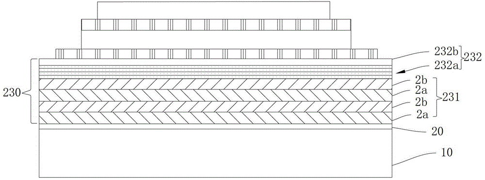
[0086] The difference between this embodiment and Embodiment 1 lies in the adhesive layer and the heat insulating support structure. like figure 2 As shown, the thermal insulation layer 231 in this embodiment includes sequentially depositing SiO from bottom to top in a direction away from the substrate 10 2 Nanoarray 2a, TiO 2 Nanoarray 2b, SiO 2 Nanoarray 2a and TiO 2 Nanoarray 2b; and SiO 2 Nanoarray, TiO 2 The tilt directions of the nanoarrays are opposite, making the SiO 2 Nanoarray TiO 2 The nanoarrays are arranged in a "zigzag" shape. Composition SiO 2 Nanoarray, TiO 2 The nano-units of the nano-array are all oblique rod-shaped.

[0087] The deposition steps of the adhesive layer 20 in this embodiment are as follows: using the electron beam deposition method, controlling the deposition angle to 0°, the deposition rate to 0.2 nm / s, and depositing a layer of HfO with a thickness of 20 nm on the Si substrate 10 2 as the adhesive layer 20 .

[0088] The preparat...

Embodiment 3

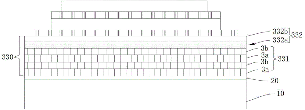
[0095] The difference between this embodiment and Embodiment 1 lies in the adhesive layer and the heat insulating support structure. like image 3 As shown, the thermal insulation layer 331 in this embodiment includes sequentially depositing SiO from bottom to top in a direction away from the substrate 2 Nanoarray 3a, TiO 2 Nanoarray 3b, SiO 2 Nanoarray 3a and TiO 2 Nanoarray 3b; and SiO 2 Nanoarray, TiO 2 The nano-arrays are arranged in a columnar shape and are perpendicular to the surface of the substrate.

[0096] The deposition steps of the adhesive layer 20 in this embodiment are as follows: using the electron beam deposition method, controlling the deposition angle to 0°, the deposition rate to 0.2 nm / s, and depositing a layer of SiO with a thickness of 50 nm on the Si substrate 10 2 as the adhesive layer 20 .

[0097] The preparation method of the thermal insulation layer 331 of the present embodiment is as follows:

[0098] (i) Adjust the deposition angle to 86...


PUM


Abstract

The invention relates to the technical field of detectors, in particular to a pyroelectric thin film infrared focal plane detector chip. The pyroelectric thin film infrared focal plane detector chip sequentially comprises a substrate, a bond coat, a heat insulation supporting structure, a lower electrode, a photosensitive element, an upper electrode and an infrared absorbing layer from bottom to top. The heat insulation supporting structure comprises a thermal insulating layer and a transition supporting layer formed on the surface of the thermal insulating layer, wherein the thermal insulating layer comprises SiO2 nanometer arrays and TiO2 nanometer arrays, and the SiO2 nanometer arrays and the TiO2 nanometer arrays are alternatively stacked up and down; the transition supporting layer comprises a plurality of SiO2 transition structures and HfO2 films deposited on the surfaces of the SiO2 transition structures, the SiO2 transition structures are sequentially stacked from bottom to top, and the porosity of the transition supporting layer gradually reduces from bottom to top. The pyroelectric thin film infrared focal plane detector chip is simple in preparation method, the porosity of the heat insulation supporting structure is flexibly adjusted, thermal conductivity of the detector chip is effectively reduced, and sensitivity, stability and reliability of a detector are meanwhile improved except that stress releasing requirements for the heat insulation supporting structure of the detector are met.

Description

technical field [0001] The invention relates to the technical field of infrared detection, in particular to a kind of high-efficiency and reliable SiO 2 and TiO 2 A thermal insulation support structure for a pyroelectric infrared focal plane detector of a composite material and a composite structure and a manufacturing method thereof. Background technique [0002] Pyroelectric thin film infrared focal plane detector has the advantages of operating frequency at room temperature, wide spectral response, fast response speed, high detection rate, can significantly improve sensor integration, and high cost performance. It is used in infrared night vision, infrared guidance, infrared imaging. , and the use of infrared focal plane detectors for firefighting and emergency rescue and other military and civilian fields have broad applications. The sensitivity of the pyroelectric thin film infrared focal plane detector mainly depends on the pyroelectric coefficient of the photosensit...

Claims


Application Information

Patent Timeline
Patent Type & Authority Patents(China)
IPC IPC(8): H01L37/02H01L37/00
Inventor 朱煜褚君浩张耀辉宋贺伦王建禄孟祥建孙硕
Owner SUZHOU INST OF NANO TECH & NANO BIONICS CHINESE ACEDEMY OF SCI
Why Eureka
Try Eureka