Back bonding platform for superchip

A high-density, chip technology, used in electrical components, circuits, semiconductor/solid-state device manufacturing, etc., can solve problems such as chip damage, alignment failure, chip pressure, etc., to facilitate control, improve positioning accuracy, and bond pressure. uniform effect

Active Publication Date: 2013-10-23
HUAZHONG UNIV OF SCI & TECH
View PDF7 Cites 72 Cited by
  • Summary
  • Abstract
  • Description
  • Claims
  • Application Information

AI Technical Summary

Problems solved by technology

However, this passive leveling mechanism requires the leveling action and the bonding action to be completed at the same position, so that the chip will be under pressure during the leveling process, which is easy to cause damage to the chip; in addition, alignment failure may also be caused during the leveling process Defects

Method used


Image

  • Back bonding platform for superchip
  • Back bonding platform for superchip
  • Back bonding platform for superchip

Examples


Embodiment Construction

[0030]In order to make the object, technical solution and advantages of the present invention clearer, the present invention will be further described in detail below in conjunction with the accompanying drawings and embodiments. It should be understood that the specific embodiments described here are only used to explain the present invention, not to limit the present invention.

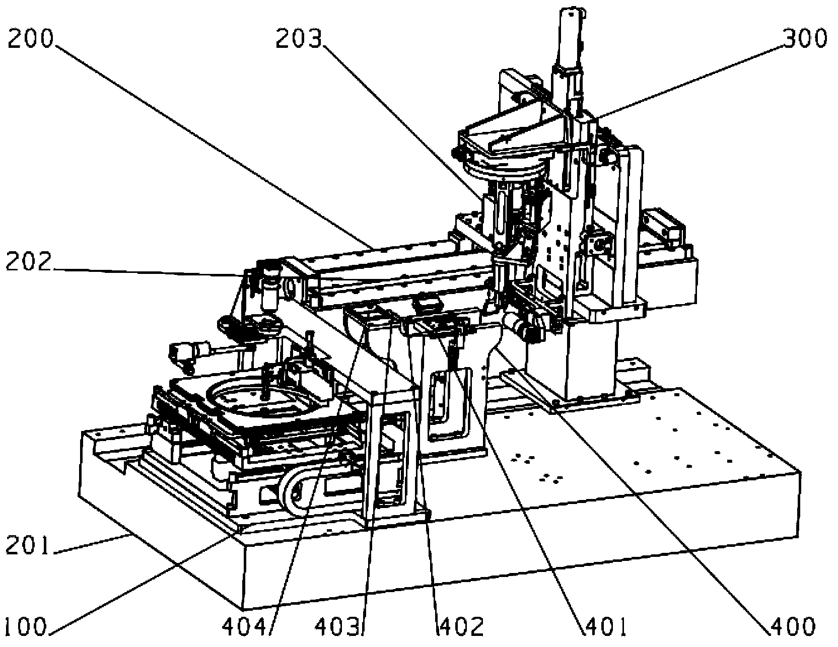
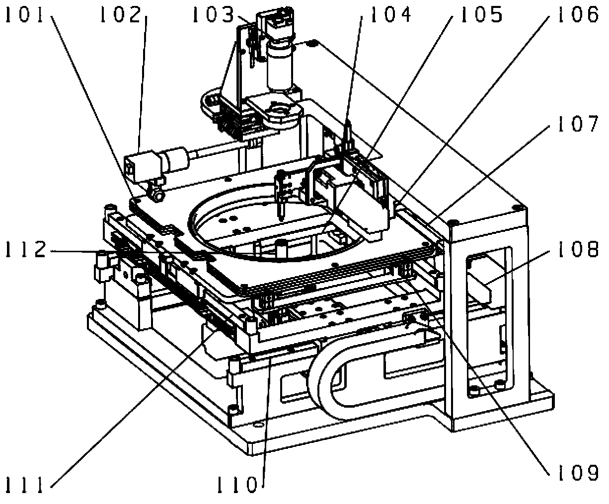
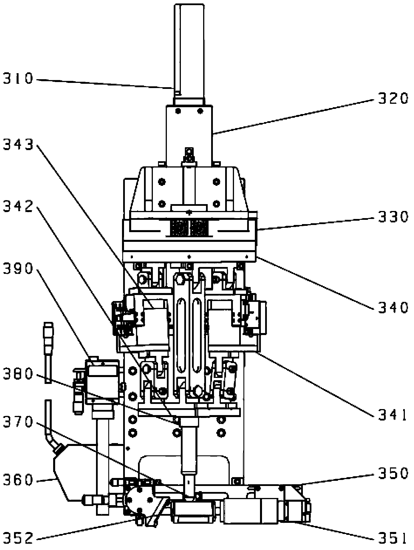
[0031] figure 1 It is a schematic diagram of the overall structure of the flip-chip bonding platform constructed according to the preferred embodiment of the present invention. Such as figure 1 As shown in , the flip-chip bonding platform according to the present invention mainly includes a base 201 as the basis for mounting all components, as well as a chip peeling and flipping unit 100, an XY direction motion unit 200, a multi-degree-of-freedom bonding head 300 and a mounting table Unit 401, through the design of the setting method of the above key components, can successfully complete operation...


PUM


Abstract

The invention discloses a back bonding platform for a superchip. The back bonding platform comprises a substrate, a chip peeling and overturning unit, an X-Y direction movement unit, a multi-degree of freedom bonding head and a mounting platform unit, wherein the chip peeling and overturning unit is used for respectively peeling and overturning a chip on a wafer disk and sending the chip to a to-be-picked position; the multi-degree of freedom bonding head is arranged on a supporting guide rail of the X-Y direction movement unit in a cantilever mode, and has functions of automatically levelling and aligning; the mounting platform unit is used for adsorbing the substrate and matched with the bonding head, so that the chip and the substrate are mutually positioned. In addition, in order to ensure the high-precision movement or matching of units, a plurality of vision positioning systems are configured in the back bonding platform. The back bonding platform can reach micrometer-level alignment accuracy, has the parallel adjusting accuracy of higher than 0.01 degree, and has the advantages of compact structure, convenience for operation and the like, so that the back bonding platform is particularly suitable for back bonding of the superchip.

Description

technical field [0001] The invention belongs to the technical field of semiconductor packaging, and more specifically relates to a flip-chip bonding platform for high-density chips. Background technique [0002] Chip flip-chip bonding technology is a method of preparing connection bumps on the bare chip electrodes, and interconnecting the bumps with the packaging substrate by brazing, hot pressing and other processes with the chip electrodes facing down. Compared with wire bonding technology, flip chip bonding has the advantages of high precision, small footprint of hybrid integrated chips, high I / O density, short interconnection wires, and small lead parasitic parameters. It has become one of the mainstream technologies in the field of chip packaging today. [0003] For some flip-chip bonding equipment that has been developed in the prior art, such as the thermosonic flip-chip bonding machine developed by Central South University, the maximum number of bumps is 40, and the...

Claims


Application Information

Patent Timeline
Patent Type & Authority Applications(China)
IPC IPC(8): H01L21/67H01L21/603
Inventor 陈建魁李宏举尹周平蔡伟林钟强龙孙湘成陈伟张步阳谢俊马亮吴沛然温雯杨航张前于明浩王冠史明辉
Owner HUAZHONG UNIV OF SCI & TECH
Why Eureka
Try Eureka