Impedance matching method, impedance matching system, and plasma processing device

A technology of impedance matching and impedance matching network, which is applied in the field of microelectronics, can solve the problems of low efficiency, difficult impedance matching, and low reliability of impedance matching, and achieve the effect of simplifying the matching process, reducing difficulty, and reliable matching

Active Publication Date: 2013-10-30
BEIJING NAURA MICROELECTRONICS EQUIP CO LTD
View PDF4 Cites 12 Cited by
  • Summary
  • Abstract
  • Description
  • Claims
  • Application Information

AI Technical Summary

Problems solved by technology

The input impedance of the impedance matching network includes the real part of the input impedance and the imaginary part of the input impedance. Therefore, it is difficult to achieve impedance matching by adjusting the transformer turns ratio and inductance L (or capacitance C), the efficiency is low, and the reliability of impedance matching is low

Method used


Image

  • Impedance matching method, impedance matching system, and plasma processing device
  • Impedance matching method, impedance matching system, and plasma processing device
  • Impedance matching method, impedance matching system, and plasma processing device

Examples


Embodiment Construction

[0050] In order for those skilled in the art to better understand the technical solution of the present invention, the impedance matching system, impedance matching method and plasma processing equipment provided by the present invention will be described in detail below with reference to the accompanying drawings.

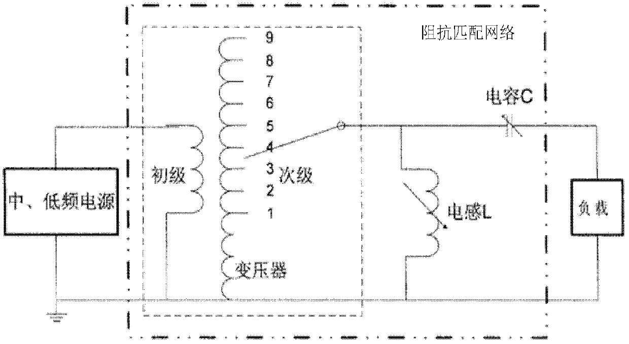
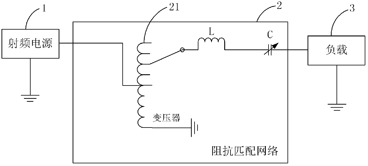
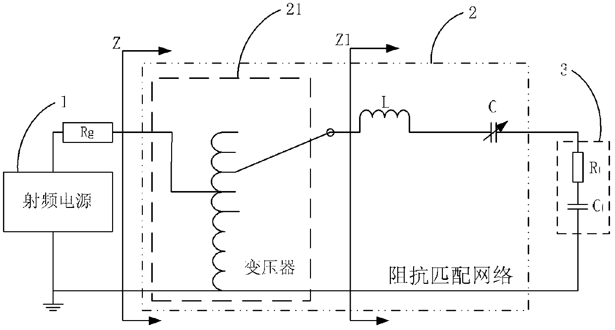
[0051] figure 2 It is a schematic structural diagram of an impedance matching system provided in Embodiment 1 of the present invention, image 3 for image 3 Equivalent circuit diagram of the medium impedance matching system. Please also refer to figure 2 and image 3 , the impedance matching system includes: an impedance matching network 2, which is arranged between the radio frequency power supply 1 and the load 3, and is used for conjugate matching the input impedance of the impedance matching network 2 and the output impedance of the radio frequency power supply 1.

[0052] The impedance matching network 2 includes: a transformer 21 , an inductor L and a...


PUM


Abstract

The invention discloses an impedance matching method, an impedance matching system, and a plasma processing device. According to the impedance matching method, impedance matching between a radio frequency power supply and a load is achieved through an impedance matching network. The impedance matching network includes: a transformer, an inductor, and a capacitor. The primary of the transformer is connected with the radio frequency power supply. The inductor, the capacitor and the load are connected serially with the secondary of the transformer in sequence. The impedance matching method includes: obtaining a turns ratio adjustment amount according to an impedance real part deviation, and adjusting the turns ratio of the transformer according to the turns ration adjustment amount; and obtaining a capacitor adjustment amount according to an impedance imaginary?part deviation, and adjusting the capacitor according to the capacitor adjustment amount. With the impedance matching method, difficulty for impedance matching is reduced so that impedance matching can be achieved easily.

Description

technical field [0001] The invention relates to the technical field of microelectronics, in particular to an impedance matching method, an impedance matching system and plasma processing equipment. Background technique [0002] Plasma equipment is widely used in the manufacturing processes of semiconductors, solar cells, and flat panel displays, such as thin film deposition or plasma etching using plasma equipment. At present, there are many ways to generate plasma, and the power applied when generating plasma is output by the power supply. The power supply usually includes DC power supply, radio frequency power supply and microwave power supply in terms of frequency bands. Among them, the radio frequency power supply can specifically include: low frequency (30kHz- 300kHz) power supply, intermediate frequency (300kHz-2MHz) power supply, high frequency (2MHz-30MHz) power supply and ultra-high frequency (30MHz-300MHz) power supply. The RF power supply itself has a characteris...

Claims


Application Information

Patent Timeline
Patent Type & Authority Applications(China)
IPC IPC(8): H01J37/32H03H7/38
Inventor 韦刚武晔
Owner BEIJING NAURA MICROELECTRONICS EQUIP CO LTD
Why Eureka
Try Eureka