

A kind of low voltage diode and its manufacturing method
A manufacturing method and diode technology, applied in semiconductor/solid-state device manufacturing, circuits, electrical components, etc., can solve problems such as increased formation defects and poor performance of diodes, so as to simplify the process, improve production efficiency, and reduce unstable product quality Effect
Active Publication Date: 2017-04-05
BEIJING YANDONG MICROELECTRONICS
View PDF3 Cites 0 Cited by
- Summary
- Abstract
- Description
- Claims
- Application Information
AI Technical Summary
Problems solved by technology
The introduction of multiple process steps increases the likelihood of defects forming in the product, which in turn increases the likelihood of chip scrapping
This defect may cause poor performance of the diode
Method used
View moreImage
Smart ImageViewing Examples

Examples
example
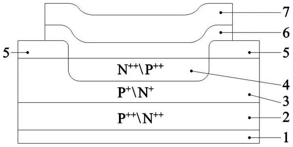
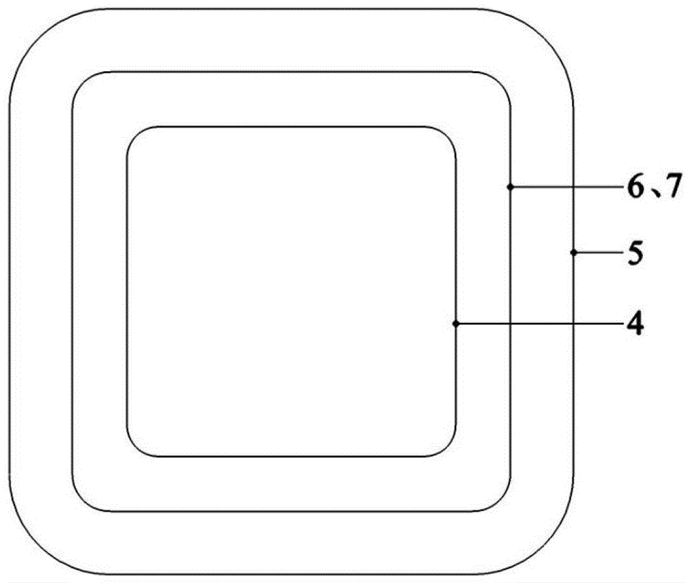
[0067] Using the above-mentioned manufacturing method, make a size of 0.2×0.2mm, the reverse breakdown voltage is 5.8V≤VR≤7.6V, when VR=5V, the leakage current IR≤100nA, can discharge the surge current Ipp ≥10A, low voltage diode with antistatic level up to 8kV. In this diode, the doping type of the epitaxial region is P-type, the resistivity is about 0.015-0.02Ω·cm, the thickness is about 6 μm, the doping type of the inverse doping active region is N-type, and the doping dose is about 1× 10 15 cm -2 , with a depth of about 1 μm. The material of the front metal electrode layer is aluminum, and the interlayer protective layer is a nickel-chromium metal layer with a thickness of 1.5 μm.
Login to View More PUM
| Property | Measurement | Unit |
|---|---|---|
| thickness | aaaaa | aaaaa |
| electrical resistivity | aaaaa | aaaaa |
| thickness | aaaaa | aaaaa |
Abstract
The invention relates to a low-voltage diode and a manufacturing method of the low-voltage diode. The method includes the following steps of forming an insulating layer with an opening on an epitaxial layer of a first conduction type, forming a high-concentration doped area of a second conduction type in the epitaxial layer by taking the insulating layer as a covering film to form a PN junction with the epitaxial layer, conducting sedimentation to sequentially form an interlayer protective layer and a metal layer on the surface of the obtained structure, conducting etching on the metal layer to obtain an electrode layer of the diode, selecting an etching agent with a high selection ratio, and taking the electrode layer as a covering film to conduct selective etching on the interlayer protective layer so that the etched interlayer protective layer can have an outer boundary which is the same as that of the electrode layer. According to the low-voltage diode manufactured through the manufacturing method, not only is the product percent of pass remarkably improved, but also the manufacturing process is simplified, and productive efficiency is correspondingly improved.
Description
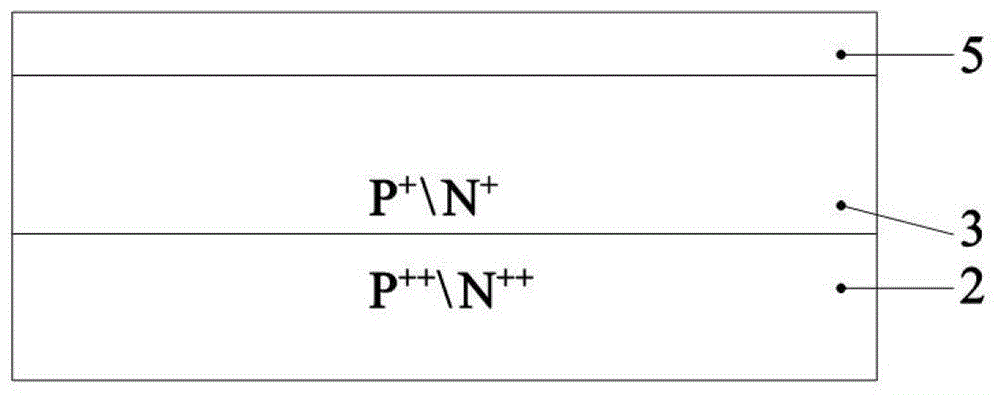
technical field [0001] The present invention relates to low voltage diode devices. More specifically, the present invention relates to a process-optimized low-voltage diode and a manufacturing method thereof. Background technique [0002] At present, in the production process of low-voltage diode chips, silicon substrates with fixed resistivity are generally used, such as: P + ,P ++ , N + or N ++ Substrate silicon substrate. The main steps of the production process include growing an epitaxial layer with a specific thickness, resistivity and doping type on the selected substrate silicon substrate, for example: in P ++ Growth of 10 μm P on the substrate silicon substrate + an epitaxial layer; doping a certain amount of impurities of the opposite conductivity type in the epitaxial layer to form a PN junction barrier; and covering the lead hole with a metal electrode layer to form an ohmic contact as an extraction electrode. Such a process mainly has two disadvantages. F...
Claims
Login to View More Application Information
Patent Timeline
 Patent Type & AuthorityPatents(China)
IPC IPC(8): H01L21/329H01L29/861
Inventor周源
OwnerBEIJING YANDONG MICROELECTRONICS