

Semiconductor structure and manufacturing method thereof
A manufacturing method and semiconductor technology, applied in semiconductor/solid-state device manufacturing, semiconductor devices, electrical components, etc., can solve problems such as limited improvement
- Summary
- Abstract
- Description
- Claims
- Application Information
AI Technical Summary
Problems solved by technology
Method used
Image

Examples
Embodiment Construction
[0052] Embodiments of the present invention will be described in detail below with reference to the accompanying drawings. The same reference numerals are used in the drawings to designate the same or similar parts. It should be noted that the drawings have been simplified to clearly illustrate the content of the embodiments, and the dimensions and ratios in the drawings are not drawn to the same proportions as actual products, so they are not used to limit the protection scope of the present invention.
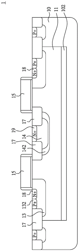
[0053] figure 1 It is a schematic diagram of a parallel laterally diffused metal oxide semiconductor (LDMOS) device according to an embodiment of the present invention. The LDMOS element 1 of the embodiment includes a P-type substrate 10, an N-type deep well (n-deep well, NDW) 11, and a highly doped N-type buried layer (n-buried layer, NBL) 102 dispersed on the substrate 10 and located below the N-type deep well 11, a P-type well 13 and an N-type well 14 are formed in the N...
PUM
 Abstract
Description
Claims
Application Information