Inductor and formation method thereof, and integrated passive device and formation method thereof

A technology for integrating passive devices and inductors, which is applied in the semiconductor field, can solve problems such as high requirements and complex structure and process of Litz wire inductors, and achieve the effects of improving quality factor, reducing loss, and increasing cross-sectional area

Inactive Publication Date: 2013-11-20
SHANGHAI HUAHONG GRACE SEMICON MFG CORP
View PDF3 Cites 7 Cited by
  • Summary
  • Abstract
  • Description
  • Claims
  • Application Information

AI Technical Summary

Problems solved by technology

Therefore, the Litz wire inductor structure has higher requirements on the layout method of each w...

Method used


Image

  • Inductor and formation method thereof, and integrated passive device and formation method thereof
  • Inductor and formation method thereof, and integrated passive device and formation method thereof
  • Inductor and formation method thereof, and integrated passive device and formation method thereof

Examples


Embodiment Construction

[0039] As mentioned in the background section, the quality factor of the existing planar inductor structure is low. Although the quality factor of the litz wire inductor structure is high, the layout requirements for each wire in the litz wire inductor structure are high, and the process of forming the litz wire inductor structure is complicated.

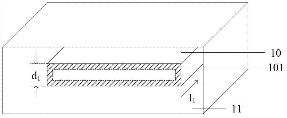
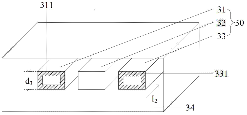
[0040]After research, it is found that the metal layer under the first opening can be removed by forming a mask layer including the first opening and the second opening on the flat metal layer, and etching the metal layer along the first opening and the second opening. layer, and a metal layer with a predetermined thickness remains under the second opening to form an inductor. The formed inductor includes a body and a plurality of spaced apart flanges located on the upper surface of the body. The surface area of ​​the inductor including the body and the flange is larger compared to the flat metal layer. Since one end of each flange...


PUM


Abstract

The invention discloses an inductor and a formation method thereof, and an integrated passive device and a formation method thereof. The formation method of the inductor comprises the steps of providing a semiconductor substrate; forming a first medium layer on the semiconductor substrate; forming a metal layer on the first medium layer; forming a mask layer on the metal layer, and forming a first opening and a second opening in the mask layer, wherein the size of the first opening is greater than the size of the second opening; etching the metal layer along the first opening and the second opening until the first medium layer below the first opening is exposed, and leaving the metal layer at predetermined thickness at the bottom of the second opening; removing the mask layer. According to the invention, a quality factor of the inductor in each frequency of an alternating current circuit is improved, the peak value of the quality factor of the inductor is larger, an auto-resonance frequency is larger, and the performance of the integrated passive device comprising the formed inductor is better.

Description

technical field [0001] The invention relates to the technical field of semiconductors, in particular to an inductor and a forming method thereof, an integrated passive device and a forming method thereof. Background technique [0002] A radio frequency (Radio Frequency, RF for short) circuit in the prior art uses a large number of passive components, such as inductors. The miniaturization of passive devices and passive device circuits is an important indicator of radio frequency device technology. [0003] Recent advances in passive device technology have resulted in Integrated Passive Devices (IPDs) in which inductors, capacitors, and resistors are integrated on a single substrate. In these IPDs, one of the goals that the design of the inductance component usually needs to achieve is a high quality factor (Quality Factor), that is, the loss of the input signal is small. [0004] refer to figure 1 , figure 1 It is an equivalent circuit diagram when an inductor is connect...

Claims


Application Information

Patent Timeline
IPC IPC(8): H01L23/64H01L21/02H01L27/01H01L21/70
Inventor 黎坡
Owner SHANGHAI HUAHONG GRACE SEMICON MFG CORP
Why Eureka
Try Eureka