Band gap reference voltage source
A reference voltage source, reference technology, applied in the direction of adjusting electrical variables, control/regulating systems, instruments, etc., to achieve the effect of saving layout area, simple circuit structure, and improving accuracy
- Summary
- Abstract
- Description
- Claims
- Application Information
AI Technical Summary
Problems solved by technology
Method used
Image

Examples
Embodiment
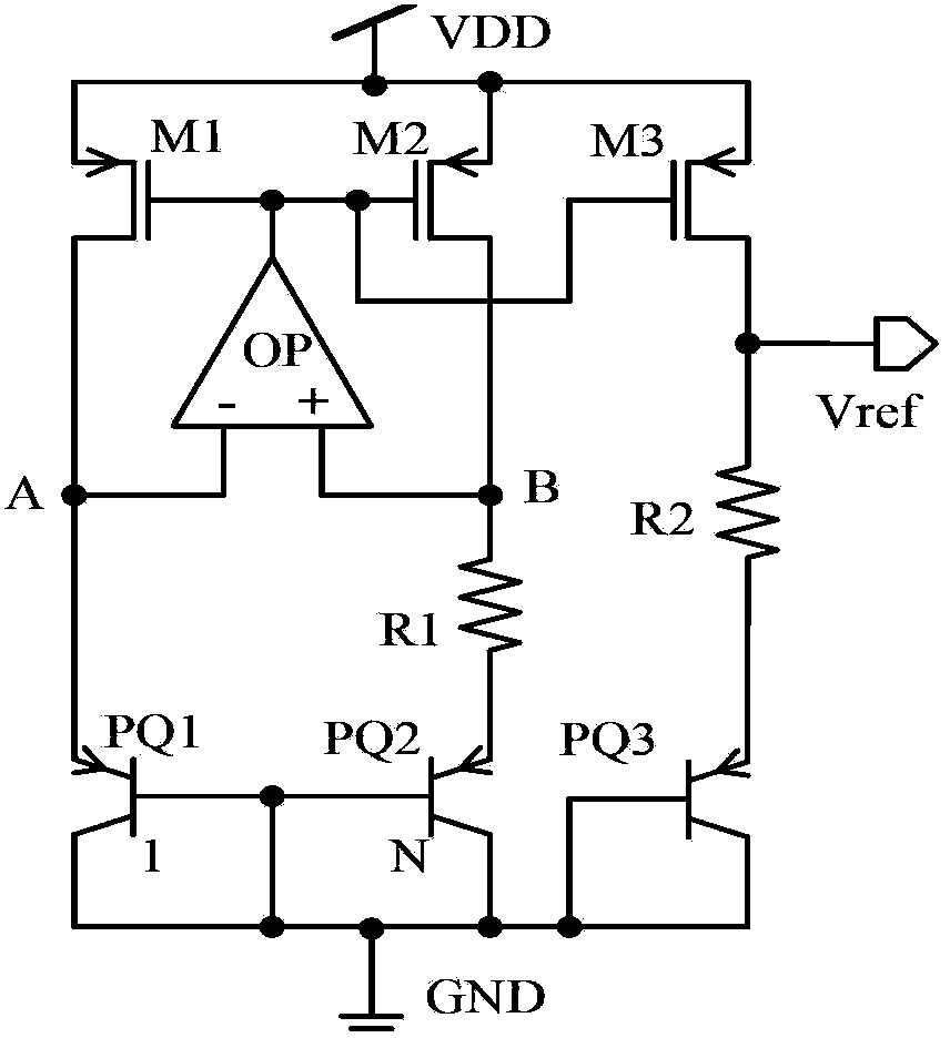
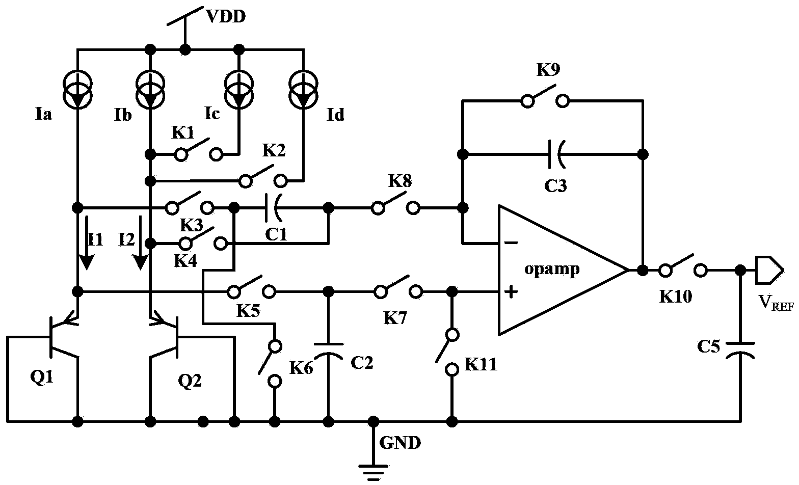
[0033] This example is a specific embodiment according to the above principle of the present invention, in image 3 basis, all switches are implemented using NMOSFETs, such as Figure 4 As shown, the bias circuit includes a first PMOS transistor P1, a second PMOS transistor P2, a third PMOS transistor P3, a fourth PMOS transistor P4, a first NMOS transistor N1, a second NMOS transistor N2, and a third NMOS transistor N3 , the fourth NMOS transistor N4, the fifth NMOS transistor N5 and the sixth NMOS transistor N6, the bandgap reference core circuit includes the fifth PMOS transistor P5, the sixth PMOS transistor P6, the first PNP type bipolar transistor Q1 and the second PNP type double-click transistor Q2, the temperature detection circuit includes a seventh PMOS transistor P7, an eighth PMOS transistor P8, a ninth PMOS transistor P9, a tenth PMOS transistor P10, an eleventh PMOS transistor P11, a twelfth PMOS transistor P12, The seventh NMOS transistor N7, the eighth NMOS t...
PUM
 Abstract
Description
Claims
Application Information
 - R&D
- Intellectual Property
- Life Sciences
- Materials
- Tech Scout
- Unparalleled Data Quality
- Higher Quality Content
- 60% Fewer Hallucinations
Browse by: Latest US Patents, China's latest patents, Technical Efficacy Thesaurus, Application Domain, Technology Topic, Popular Technical Reports.
© 2025 PatSnap. All rights reserved.Legal|Privacy policy|Modern Slavery Act Transparency Statement|Sitemap|About US| Contact US: help@patsnap.com