Node device of sensing network capable of supporting sensing access and optical packet transmission
A sensor network and optical grouping technology, applied in optical fiber transmission, transmission systems, digital transmission systems, etc., can solve the problem that the signal processing bit rate cannot meet the needs of high-speed and large-capacity data interaction, and achieve improved data exchange capabilities, The effect of reducing protocol overhead, complexity and cost
- Summary
- Abstract
- Description
- Claims
- Application Information
AI Technical Summary
Problems solved by technology
Method used
Image
Examples
Embodiment 1
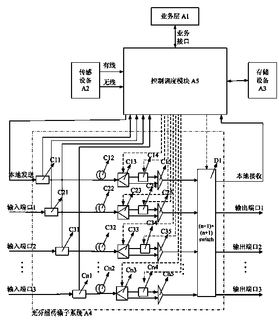
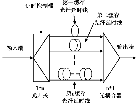
[0027] A node device of a sensor network supporting sensor access and optical packet transmission, such as figure 1 shown. Including business layer A1, sensing device A2, storage device A3, optical packet transmission subsystem A4 and control scheduling module A5, business layer A1 and control scheduling module A5 are connected through service interfaces, sensing device A2 and control scheduling module A5 are connected through wired The wireless transmission interface is connected, the storage device A3 is connected with the control scheduling module A5 through the address data bus, and the optical packet transmission subsystem A4 includes n+1 switching branches, n is a positive integer not greater than 16, and (n+1 )*(n+1) gating optical switch D1, the output ends of n+1 switching branches are respectively connected to n+1 input ends of (n+1)*(n+1) gating optical switch D1, One input terminal in the n+1 switching branches is connected to the local sending port of the control...
Embodiment 2
[0036] The structure of the sensor network is as Figure 5 As shown, the optical packet transmission subsystem A4 is used to transmit and connect the nodes in the sensor network with other nodes, thereby forming a transmission network.
[0037] The sensing interface of the node device such as Image 6 As shown, it includes XC5VLX50T FPGA chip E1, PCIE interface E2, KM62256C SRAM E3, XCF16PVO48C PROM E4, Ethernet interface E5, optical fiber interface E6, USB interface E8, ZigBee interface E9, WIFI interface E10. PCIE interface E2, KM62256C static random access memory E3, XCF16PVO48C programmable read-only memory E4, Ethernet interface E5, optical fiber interface E6, USB interface E8, ZigBee interface E9, WIFI interface E10 are respectively connected to XC5VLX50T FPGA chip E1. Among them, the PCIE interface E2 is a business interface, which is developed by the ip core of Xilinx Company. KM62256C static random access memory E3 and XCF16PVO48C programmable read-only memory E4 be...
Embodiment 3
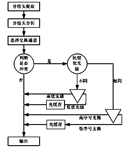
[0041] Conflict resolution algorithm for output signals of node devices, such as image 3 shown.
[0042] When there are six optical packet signals arriving from the input ports of the first switching branch to the sixth switching branch at the same time, the priorities of the optical packet signals from the first switching branch to the sixth switching branch are respectively 2, 1, 2, 2, 3, 4, wherein the optical packet signal of the first switching branch should reach the output port 1, and the remaining optical packet signals should reach the output port 2, then the optical packet signal of the first switching branch has no conflict and can be directly output to the target port.
[0043] The optical packet signals of the second to sixth switching branches conflict, and the control scheduling module controls the 1*2 optical switch of the sixth switching branch, so that the high-priority optical packet signals with the priority of 4 in the sixth switching branch can be direc...
PUM
 Abstract
Description
Claims
Application Information


