
Solar cell and manufacturing method thereof

A technology of solar cells and manufacturing methods, applied in the field of solar cells, can solve problems such as lattice mismatch, achieve the effects of increasing yield, avoiding cracks and falling off, and improving quality

Active Publication Date: 2013-12-04
SUZHOU INST OF NANO TECH & NANO BIONICS CHINESE ACEDEMY OF SCI
View PDF5 Cites 23 Cited by
  • Summary
  • Abstract
  • Description
  • Claims
  • Application Information

AI Technical Summary

Problems solved by technology

However, too many material systems used on the same substrate will cause serious lattice mismatch.

Method used


Image

  • Solar cell and manufacturing method thereof
  • Solar cell and manufacturing method thereof
  • Solar cell and manufacturing method thereof

Examples


Embodiment 1

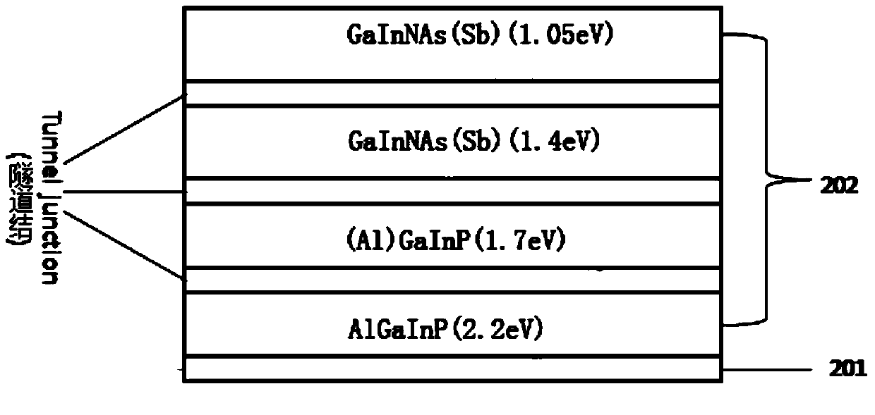
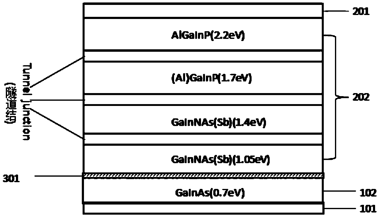
[0036] ginseng Figure 5 As shown, the solar cell includes a substrate 101, a GaInAs-based cell film layer 102 formed above the substrate 101, and a GaInAs-based cell film layer bonded AlGaInP / (Al)GaInP / GaInNAs(Sb) / GaInNAs(Sb) four-junction The battery film layer 202 further includes two electrodes electrically connected to the AlGaInP layer and the GaInAs-based battery film layer respectively.

[0037] The substrate 101 is an InP substrate, and may also be other substrates such as silicon, metal, or plastic.

[0038] The GaInAs-based battery film layer 102 and the AlGaInP / (Al)GaInP / GaInNAs(Sb) / GaInNAs(Sb) four-junction battery film layer 202 are bonded through the metal thin film layer 301 . In other embodiments, direct bonding methods such as eutectic, high temperature treatment, or electrostatic bonding may also be used between the two, and an inverted soldering process may also be used.

[0039] AlGaInP / (Al)GaInP / GaInNAs(Sb) / GaInNAs(Sb) four-junction cell film layer 202 ...

Embodiment 2

[0057] ginseng Figure 6 As shown, the solar cell includes a substrate 101, a GaInAs-based cell film layer 102 formed above the substrate 101, and a GaInAs-based cell film layer bonded AlGaInP / (Al)GaInP / GaInNAs(Sb) / GaInNAs(Sb) four-junction The battery film layer 202, the GaInAs-based battery film layer and the AlGaInP / (Al)GaInP / GaInNAs(Sb) / GaInNAs(Sb) four-junction battery film layer all adopt a double-layer mesa structure, and the GaInAs-based battery film layer and the AlGaInP / An electrode 401 , 402 , 403 and 403 is provided on the exposed surface of each mesa structure in the (Al)GaInP / GaInNAs(Sb) / GaInNAs(Sb) four-junction battery film layer. .

[0058] The substrate 101 is an InP substrate, and may also be other substrates such as silicon, metal, or plastic.

[0059] The GaInAs-based battery film layer 102 and the AlGaInP / (Al)GaInP / GaInNAs(Sb) / GaInNAs(Sb) four-junction battery film layer 202 are bonded through the metal thin film layer 301 . In other embodiments, dire...

no. 2 Embodiment

[0068] This embodiment provides a method for bonding an integrated GaInAs-based battery film layer 102 with an AlGaInP / (Al)GaInP / GaInNAs(Sb) / GaInNAs(Sb) four-junction battery film layer 202 and preparing a four-electrode terminal. The preparation process includes:

[0069] Step 1: Grow a GaInAs-based battery film layer 102 on an InP substrate 101 by MBE or MOCVD, and grow an AlGaInP / (Al)GaInP / GaInNAs(Sb) / GaInNAs(Sb) four-junction inverted on the GaAs substrate 201 Battery film layer 202 .

[0070] Step 2: Bond the GaInNAs(Sb) surface of the AlGaInP / (Al)GaInP / GaInNAs(Sb) / GaInNAs(Sb) four-junction battery film layer 202 to the exposed surface of the GaInAs-based battery film layer 102 by wafer bonding technology.

[0071] After the AlGaInP / (Al)GaInP / GaInNAs(Sb) / GaInNAs(Sb) four-junction battery film layer 202 and the GaInAs-based battery film layer 102 were respectively organically cleaned, they were soaked in a hydrogen fluoride solution with a volume ratio of 7:100 for 30 se...


PUM


Abstract

The invention discloses a solar cell which comprises a substrate, a GaInAs base cell film layer and an AlGaInP / (Al)GaInP / GaInNAa(Sb) / GaInNAs(Sb) four-junction cell film layer, wherein the GaInAs base cell film layer is formed on the surface of the substrate, and the four-junction cell film layer is bonded with the GaInAs base cell film layer. The invention further discloses a manufacturing method of the solar cell. Compared with a traditional cell, the solar cell integrates the GaInAs base cell film layer and the AlGaInP / (Al)GaInP / GaInNAa(Sb) / GaInNAs(Sb) four-junction cell film layer, and a five-junction efficient low-cost laminated solar cell structure formed after bonding is more effectively matched with solar spectra, so that cell conversion efficiency is improved.

Description

technical field [0001] The application belongs to the field of solar cells, in particular to a five-junction laminated cell containing GaInNAs (Sb) sub-cells and a preparation method thereof. Background technique [0002] The solar spectrum is a broad spectrum, and the photon energy range is about 0~4eV, so it fundamentally determines that the conversion efficiency of single-junction solar cells is lower than that of the corresponding monochromatic spectrum (photon energy is greater than the bandgap width). The solution is also very simple. In principle, instead of converting all photon energy with a solar cell with a fixed band gap, it is better to divide the spectrum into several regions and use several junctions in multi-junction solar cells with matching band gaps. area for photoelectric conversion. Assume that the energy of the spectrum is divided into several regions hν 1 ~hν 2 , hν 2 ~hν 3 , hν 3 ~hν ∞ , where hν 1 <hν 2 <hν 3 , then the bandgaps of ea...

Claims


Application Information

Patent Timeline
Patent Type & Authority Applications(China)
IPC IPC(8): H01L31/0687H01L31/0693H01L31/0224H01L31/18
CPCY02E10/50Y02E10/544Y02P70/50
Inventor 王乃明郑新和吴渊渊甘兴源王海啸杨辉
Owner SUZHOU INST OF NANO TECH & NANO BIONICS CHINESE ACEDEMY OF SCI
Learn More