Organic light-emitting device and preparation method thereof

An electroluminescence device and luminescence technology, which are applied in the fields of electric solid-state devices, chemical instruments and methods, semiconductor/solid-state device manufacturing, etc., can solve problems such as the reduction of the recombination probability of holes and electrons, the change of color coordinates, and poor color rendering

Inactive Publication Date: 2013-12-04
OCEANS KING LIGHTING SCI&TECH CO LTD +1
View PDF5 Cites 2 Cited by
  • Summary
  • Abstract
  • Description
  • Claims
  • Application Information

AI Technical Summary

Problems solved by technology

[0004] In traditional light-emitting devices, the hole transport rate is generally more than two orders of magnitude higher than the electron transport rate, which causes a large number of holes to accumulate in the light-emitt...

Method used


Image

  • Organic light-emitting device and preparation method thereof
  • Organic light-emitting device and preparation method thereof

Examples


Embodiment 1

[0069] A method for preparing an organic electroluminescent device, comprising the following steps:

[0070] (1) Photolithographically process the ITO, cut it into the required size, and use detergent, deionized water, acetone, ethanol, and isopropanol to sonicate for 15 minutes each to remove organic pollutants on the glass surface. The anode substrate is subjected to oxygen plasma treatment, the treatment time is 5min, and the power is 30W;

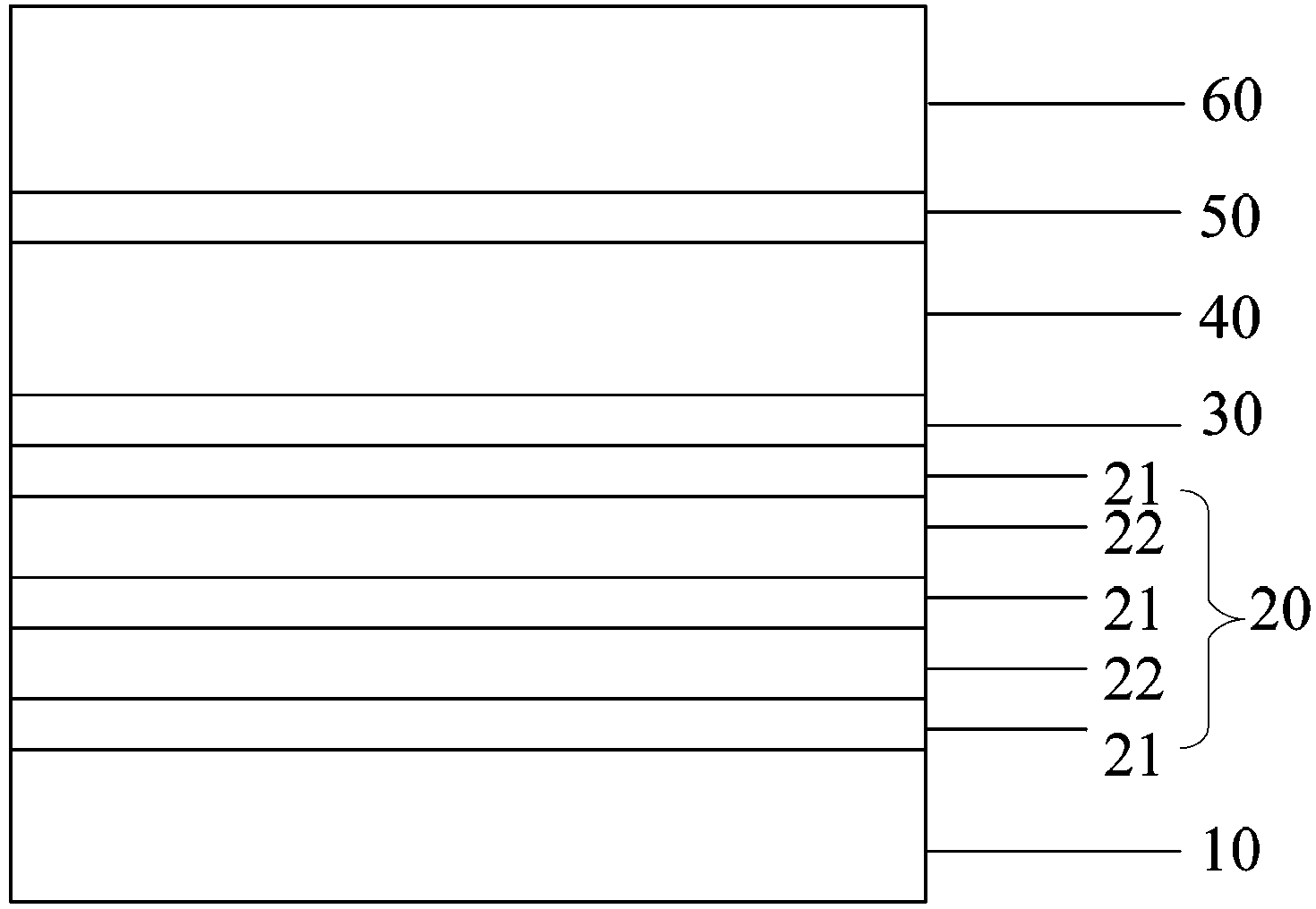
[0071] (2) Evaporating the quantum well layer on the anode substrate treated in (1), evaporating the first organic material layer on the anode substrate, and evaporating the first p-doped layer on the first organic material layer. The first p-doped layer is vapor-deposited on the first organic material layer, the second p-doped layer is vapor-deposited on the second organic material layer, the third organic material layer is vapor-deposited on the second p-doped layer, and the quantum well layer includes The first, second and third org...

Embodiment 2

[0079] A method for preparing an organic electroluminescent device, comprising the following steps:

[0080] (1) Perform photolithography treatment on IZO, cut it into the required size, and use detergent, deionized water, acetone, ethanol, and isopropanol to sonicate for 15 minutes each to remove organic pollutants on the glass surface. The anode conductive substrate is subjected to oxygen plasma treatment, the treatment time is 5min, and the power is 30W;

[0081] (2) Evaporating the quantum well layer on the anode conductive substrate treated in (1), evaporating the first organic material layer on the anode conductive substrate, and evaporating a p-doped layer on the first organic material layer, Then evaporate a second organic material layer on the p-doped layer, and the quantum well layer includes the first and second organic material layers and the p-doped layer.

[0082] Wherein, in this embodiment, the material of the p-doped layer is TAPC doped WO 3 Formed hybrid ma...

Embodiment 3

[0087] A method for preparing an organic electroluminescent device, comprising the following steps:

[0088] (1) Photolithographically process the ITO, cut it into the required size, and use detergent, deionized water, acetone, ethanol, and isopropanol to sonicate for 15 minutes each to remove organic pollutants on the glass surface. The anode substrate is subjected to oxygen plasma treatment, the treatment time is 5min, and the power is 30W;

[0089] (2) Evaporating the quantum well layer on the anode substrate treated in (2), evaporating the first organic material layer on the anode conductive substrate, and evaporating the first p-doped layer on the first organic material layer. The second organic material layer is evaporated on the first p-doped layer, the second p-doped layer is evaporated on the second organic material layer, the third organic material layer is evaporated on the second p-doped layer, and the third organic material layer is evaporated on the third p-doped...


PUM

PropertyMeasurementUnit
Thicknessaaaaaaaaaa
Thicknessaaaaaaaaaa
Thicknessaaaaaaaaaa

Abstract

An embodiment of the invention discloses an organic light-emitting device. The organic light-emitting device comprises an anode, a light-emitting layer, an electron transport layer, an electron injection layer and a cathode and further comprises a quantum well layer formed between the anode and the light-emitting layer. The quantum well layer comprises at least two layers of organic material layers stacked in sequence and a p-type doping layer arranged between the two layers of adjacent organic material layers, the p-type doping layer is made of a mixed material formed by enabling a hole transport material to be doped with a metal oxide, the doping mass fraction of the metal oxide in the p-type doping layer is 10-40%, and the organic material layers are made of organic materials with the highest occupied molecular orbital (HOMO) energy level ranging from -6.5Ev to -5.5eV. In addition, the embodiment of the invention further discloses a preparation method of the organic light-emitting device. According to the organic light-emitting device, the hole and electron recombination probability is effectively improved by adjusting the hole transporting speed, and the goal of improving light-emitting efficiency is achieved finally.

Description

technical field [0001] The invention relates to the related field of electronic devices, in particular to an organic electroluminescent device and a preparation method thereof. Background technique [0002] In 1987, C.W.Tang and Van Slyke of Eastman Kodak Company in the United States reported a breakthrough in the research of organic electroluminescence. They used ultra-thin film technology to prepare high-brightness, high-efficiency double-layer organic electroluminescent devices (OLEDs). In this double-layer structure device, the brightness reaches 1000cd / m at 10V 2 , its luminous efficiency is 1.51lm / W, and its lifespan is more than 100 hours. [0003] The principle of OLED light emission is based on the action of an external electric field, electrons are injected from the cathode to the lowest unoccupied molecular orbital (LUMO) of the organic material compound, and holes are injected from the anode to the highest occupied orbital (HOMO) of the organic material compoun...

Claims


Application Information

Patent Timeline
IPC IPC(8): H01L51/52H01L51/54H01L51/56C09K11/06
Inventor 周明杰王平黄辉陈吉星
Owner OCEANS KING LIGHTING SCI&TECH CO LTD
Why Eureka
Try Eureka