Forming method for conductive jack of ceramic heat dissipation substrate

A technology for heat dissipation substrates and substrates, which is applied in the reinforcement of conductive patterns, the formation of electrical connections of printed components, and the secondary treatment of printed circuits. It can solve problems such as inability to penetrate the electroplating solution, trouble employees, and increase the burden on the substrate to achieve ideal heat conduction. efficiency effect

Inactive Publication Date: 2013-12-04
TA I TECH
View PDF1 Cites 15 Cited by
  • Summary
  • Abstract
  • Description
  • Claims
  • Application Information

AI Technical Summary

Problems solved by technology

[0004] If relying on several heat dissipation components to assist in heat dissipation, it will not only increase the density space of the substrate, but also increase the badness of heat dissipation, and also increase the burden on the substrate
[0005] Moreover, when producing alumina substra

Method used


Image

  • Forming method for conductive jack of ceramic heat dissipation substrate
  • Forming method for conductive jack of ceramic heat dissipation substrate
  • Forming method for conductive jack of ceramic heat dissipation substrate

Examples


Embodiment Construction

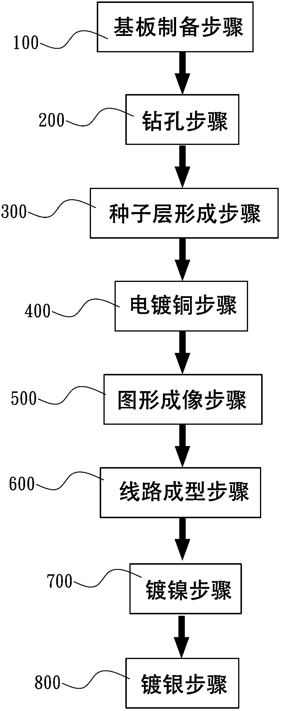
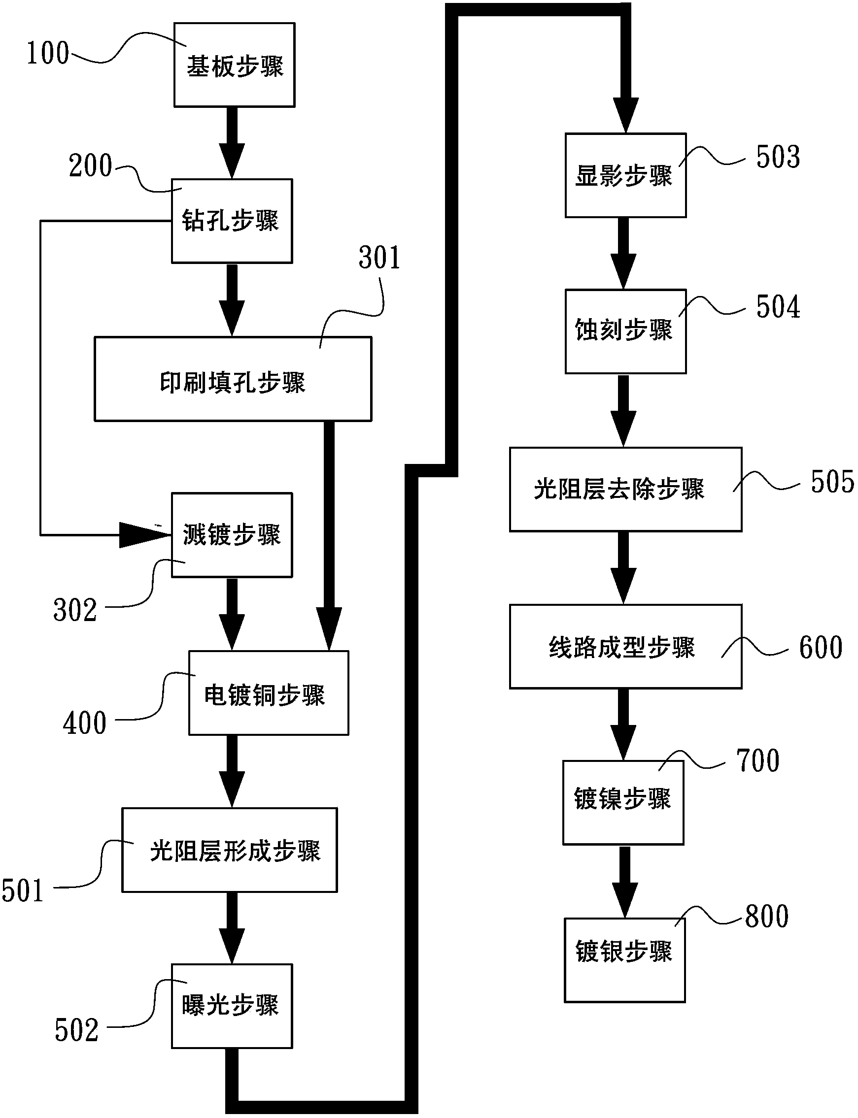
[0048] The method for forming the conductive socket of the ceramic heat dissipation substrate of the present invention can be divided into two implementation modes with and without wires. The method of forming a conductive hole of a ceramic heat dissipation substrate without a wire is as follows: figure 1 with figure 2 Shown, including:

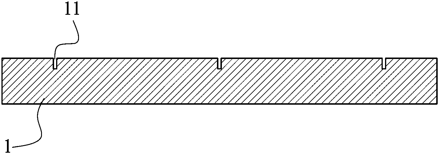
[0049] Substrate preparation step 100: select an alumina substrate or an aluminum nitride substrate as the main substrate 1, and form several cutting channels 11 on the surface of the substrate 1 (such as Figure 3A (Shown); the cutting lane 11 can be formed in the vertical direction, can also be formed in the lateral direction, so that the substrate can be broken from the cutting lane 11 to obtain a fixed size ceramic heat dissipation substrate unit;

[0050] Drilling step 200: Use laser drilling technology to drill a predetermined conductive hole position on the substrate 1 to form a hole 21 (such as Figure 3B Shown). Because the laser drillin...


PUM


Abstract

The invention relates to a forming method for a conductive jack of a ceramic heat dissipation substrate. The method comprises the following steps of a substrate preparing step, a hole drilling step, a printing silver colloid hole filling step, a sputtering coating step, an electro-coppering step, a photoresistance layer forming step, an exposing step, a development step, an etching step, a photoresistance layer removing step, a line moulding step, a nickel plating/sputter coating step, and a silver plating step. On the basis of the forming steps, a conductive jack with the advantages of ideal heat conduction efficiency, low cost, and stable physical property can be manufactured.

Description

Technical field [0001] The present invention relates to a method for forming a conductive socket on a ceramic heat dissipation substrate, in particular to a method for forming a conductive socket with ideal thermal conductivity, low cost and stable physical properties. Background technique [0002] Due to the rapid development of the electronics industry, the circuit density on the circuit board is getting higher and higher, and the waste heat accumulated on the circuit board during use is becoming less and less easy to dissipate. Nowadays, circuit boards have a trend of being lighter in terms of functional requirements, so that circuit boards are often installed in small confined spaces, and the waste heat generated during the operation process cannot be dissipated as a result, which will not only affect the operation quality of the circuit, but also It will also reduce the service life of related components. [0003] In the prior art, a heat-conducting adhesive resin is arranged...

Claims


Application Information

Patent Timeline
IPC IPC(8): H05K3/42H05K3/24
Inventor 曹茂松陈文生叶小彰黄成财杨士贤
Owner TA I TECH
Why Eureka
Try Eureka