Semiconductor material parameter tester and test method based on surface photovoltage method

A technology of surface photovoltage and material parameters, which is applied in the direction of single semiconductor device testing, etc., can solve problems such as surface damage, manpower consumption, material and power, and silicon wafer damage, so as to reduce the influence of grain boundary effects, stabilize and accurate measurement results, and avoid The effect of being destroyed

Active Publication Date: 2016-02-10
广州市昆德科技有限公司
View PDF5 Cites 2 Cited by
  • Summary
  • Abstract
  • Description
  • Claims
  • Application Information

AI Technical Summary

Problems solved by technology

Both methods have a certain scope of application, and these two methods are contact methods that use the probe to directly contact the surface of the sample. The disadvantages are: (1) the probe touches the semiconductor surface, and the surface will be damaged to a certain extent; ( 2) If the pressure is not enough, oxides on the surface of the probe and the surface of the semiconductor sample may also cause measurement errors
Therefore, the polysilicon factory consumes a lot of manpower, material resources, and electricity to test the resistivity of polysilicon, and produces waste acid and waste gas during the measurement, causing environmental pollution.
[0004] With the development of semiconductor material processing technology, semiconductor wafers are becoming thinner and thinner (the thickness of silicon wafers for solar cells has reached 160-180 μm), and the measurement of important electrical parameters such as model, resistivity / square resistance can no longer be used. The traditional three-probe, four-probe method and hot and cold pen measurement equipment, because these measurement methods must press the hard and sharp metal probes on the silicon wafer, it is easy to cause damage to the silicon wafer, and these traditional methods The method cannot adapt to the requirements of modern automatic sorting of silicon wafers

Method used


Image

  • Semiconductor material parameter tester and test method based on surface photovoltage method
  • Semiconductor material parameter tester and test method based on surface photovoltage method
  • Semiconductor material parameter tester and test method based on surface photovoltage method

Examples


Embodiment 1

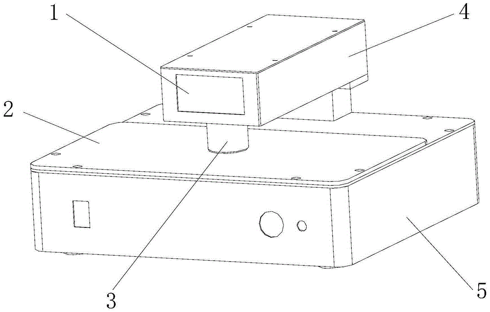
[0035] Such as figure 1 As shown, the semiconductor material parameter tester based on the surface photovoltage method in this embodiment includes a liquid crystal display 1 , a sample stage 2 , a measuring probe 3 , a cantilever 4 , and a box 5 . Among them, the sample table 2 and the cantilever 4 are set on the top of the box body 5, the measuring probe 3 and the liquid crystal display 1 are set on the cantilever 4, the center of the measuring probe 3 is aligned with the center of the sample table 2, and there is a certain gap in the middle for placing Sample to be tested.

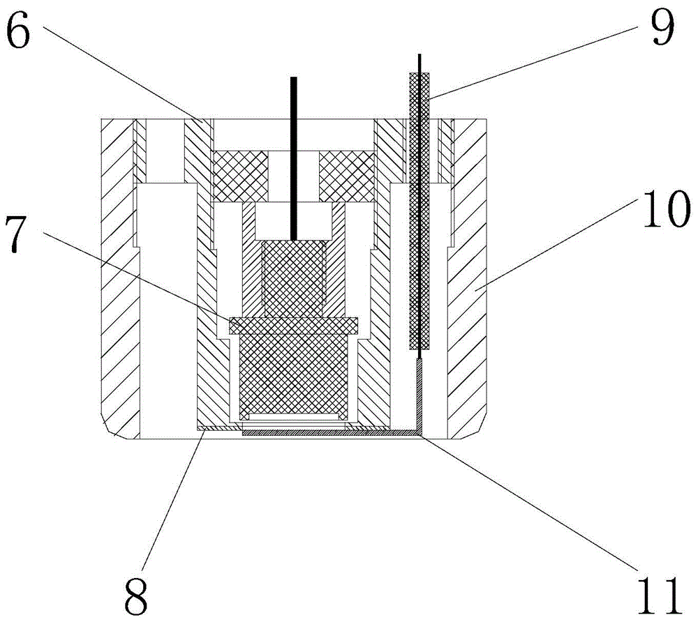
[0036] Such as figure 2As shown, the measuring probe 3 includes an aluminum alloy sleeve 6 , an infrared laser 7 , a shielding film 8 , a coaxial cable 9 , an aluminum alloy shell 10 , and an induction electrode sheet 11 . The infrared laser 7 is placed in the aluminum alloy sleeve 6, and the two are separated by a thin layer of gasket. There is a round hole on the top of the aluminum alloy sleeve 6 f...


PUM


Abstract

The invention discloses a surface photovoltage method based semiconductor material parameter testing device and testing method. The testing device comprises a casing, a cantilever, a measuring probe and a sample bench, wherein the measuring probe is internally provided with an infrared laser and a sensing electrode slice; a pulse light source driver is positioned inside the casing; a semiconductor material sample to be tested is arranged on the sampling bench; the measuring probe is right over the sample to be tested; the sensing electrode slice is connected with a charge amplifier through a coaxial cable wire; and the infrared laser is connected with the pulse light source driver through a two-core shield wire. The testing method is as follows: the pulse light emitted by the infrared laser is vertically irradiated on the sample, the sensing electrode slice receives the static charge generated by the weak photovoltage on the surface of the sample for transmitting to the input end of the charge amplifier, and a liquid crystal display screen displays the conductive type and resistivity / sheet resistance values of the sample to be tested after the static charge is processed by a signal processing circuit. The testing device provided by the invention has the advantages of small volume, light weight, small power consumption and low cost.

Description

technical field [0001] The invention relates to the research field of a semiconductor material electrical parameter tester, in particular to a semiconductor material parameter tester and a test method based on a surface photovoltage method. Background technique [0002] The conductivity type and resistivity / resistance of semiconductor materials is an important basic electrical parameter. According to whether the doped element is an acceptor or a donor element, semiconductor materials are divided into two types: P-type and N-type. Measuring the conductivity type of semiconductors can provide the original basis for manufacturing semiconductor devices. At present, there are two main methods for measuring the conductivity type of semiconductor materials at home and abroad: (1) cold and hot probe method; (2) three-probe method. The cold and hot probe method applies the principle of thermoelectric effect of semiconductor materials and is mainly suitable for the measurement of lo...

Claims


Application Information

Patent Timeline
Patent Type & Authority Patents(China)
IPC IPC(8): G01R31/26
Inventor 王昕冯小明田蕾
Owner 广州市昆德科技有限公司
Why Eureka
Try Eureka