Grid electrode LELE dual graph forming method based on DARC mask structure

A double image and mask technology, applied in the field of microelectronics, can solve the problems of not being commonly used, spending a lot of time and energy, and increasing the difficulty of controlling the uniformity of critical dimensions, so as to save costs and improve maturity and stability.

Active Publication Date: 2013-12-11
SHANGHAI HUALI MICROELECTRONICS CORP
View PDF6 Cites 6 Cited by
  • Summary
  • Abstract
  • Description
  • Claims
  • Application Information

AI Technical Summary

Problems solved by technology

[0008] Among them, when performing the above-mentioned first etching process, an advanced patterning film (APF for short) is generally used as a soft-mask (soft-mask), and when performing the second etching process, ODL is used. And SHB as a soft mask, so that the critical dimensions of the structure formed after the two etching processes are divided into two different levels, making it more difficult to control t

Method used


Image

  • Grid electrode LELE dual graph forming method based on DARC mask structure
  • Grid electrode LELE dual graph forming method based on DARC mask structure
  • Grid electrode LELE dual graph forming method based on DARC mask structure

Examples


Embodiment Construction

[0034] The specific embodiment of the present invention will be further described below in conjunction with accompanying drawing:

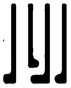
[0035] Figure 2-8 It is a schematic diagram of the process structure of an embodiment of the gate LELE double pattern forming method based on the DARC mask structure of the present invention; as Figure 2-8 As shown, a gate LELE double patterning method based on DARC mask structure is preferably applied to the gate line tail cutting process of 28 / 20 nanometers and below technology nodes on a 193nm immersion optical lithography platform , the above methods include:

[0036] First, if figure 2 As shown, on a silicon substrate (Silicon) 1, a gate oxide layer 2, a polysilicon layer (poly) 3, a silicon nitride layer (SiN) 4, an advanced pattern film layer (APF) 5 and a dielectric anti-reflection layer ( Dielectric Anti_Reflectivity Coating, referred to as DARC) 6, to form such as figure 2 The structure shown; wherein, the gate oxide layer 2, the...


PUM


Abstract

The invention relates to the technical field of microelectronics, in particular to a grid electrode LELE dual graph forming method based on a DARC mask structure. A medium anti-reflection layer hard mask structure based on an advanced graph film layer is formed through double exposure techniques, so that an APF is finally used as a mask for a polycrystalline silicon etching technique. In addition, in the second etching process of a dual graph forming technique, a DARC hard mask is used for replacing a traditional silicon oxide hard mask, a bottom layer structure ODL based on spin coating and a middle layer structure SHB, so that the technical process where the APF is used as the mask in a relatively mature 40nm technology node is continued. Therefore, cost is reduced, and the maturity and stability of a 22-namometer technology node technique and technology node techniques below 22 namometers are further improved at the same time.

Description

technical field [0001] The invention relates to the technical field of microelectronics, in particular to a gate LELE double pattern forming method based on a DARC mask structure. Background technique [0002] At present, at the technology node of 32nm and below, it is applied to the key-level lithography process. Since the resolution index required by it has exceeded the limit capability of the existing optical lithography platform, the industry has adopted a variety of technical solutions to solve the problem. This technical problem, and according to the ITRS roadmap, technical solutions such as Double Patterning Technology (DPT for short), extreme ultraviolet technology (EUV), and electronic direct writing (EBL) have been placed high expectations by the industry. [0003] Among them, double patterning technology (DPT) is expected to be used in the mass production of the 22nm photolithography process and the 28nm end-of-line cutting process in the future. The DPT technolog...

Claims


Application Information

Patent Timeline
IPC IPC(8): H01L21/28H01L21/311
Inventor 黄君毛智彪崇二敏黄海张瑜
Owner SHANGHAI HUALI MICROELECTRONICS CORP
Why Eureka
Try Eureka