

Array substrate, manufacturing method of array substrate and display device
A technology of an array substrate and a manufacturing method, which are applied in the fields of an array substrate and a manufacturing method thereof and a display device, can solve the problems of affecting the performance of TFT, the metal electrode is easily oxidized, the resistance of the metal electrode is increased, and the like, and the effect of ensuring the performance is achieved.
- Summary
- Abstract
- Description
- Claims
- Application Information
AI Technical Summary
Problems solved by technology
Method used
Image

Examples
Embodiment Construction
[0046] In order to make the technical problems, technical solutions and advantages to be solved by the embodiments of the present invention clearer, the following will describe in detail with reference to the drawings and specific embodiments.
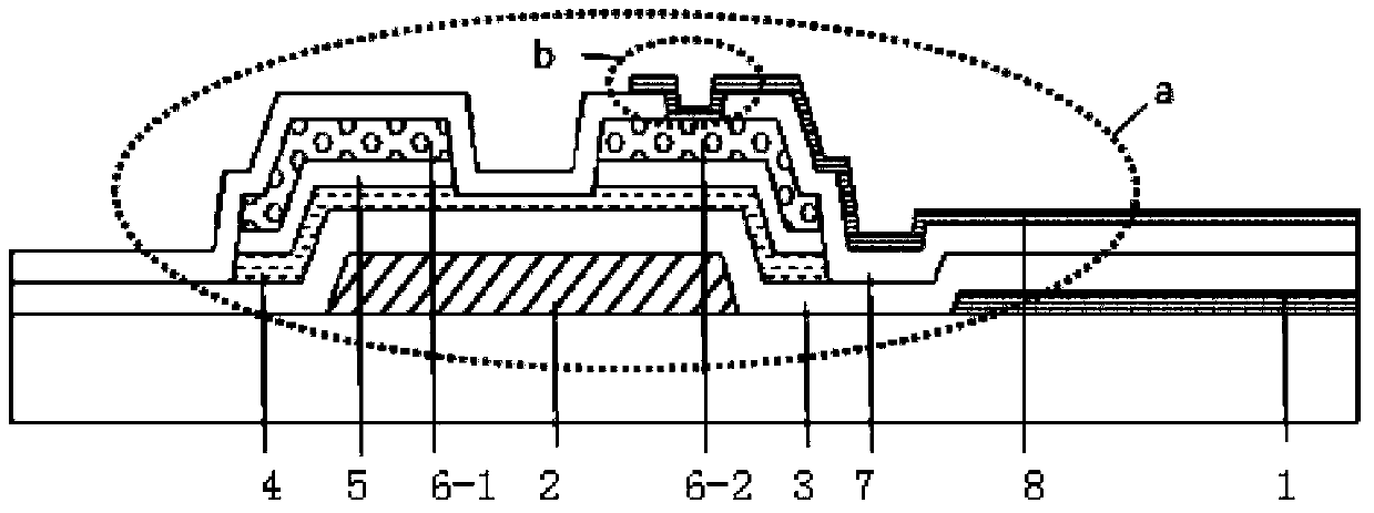
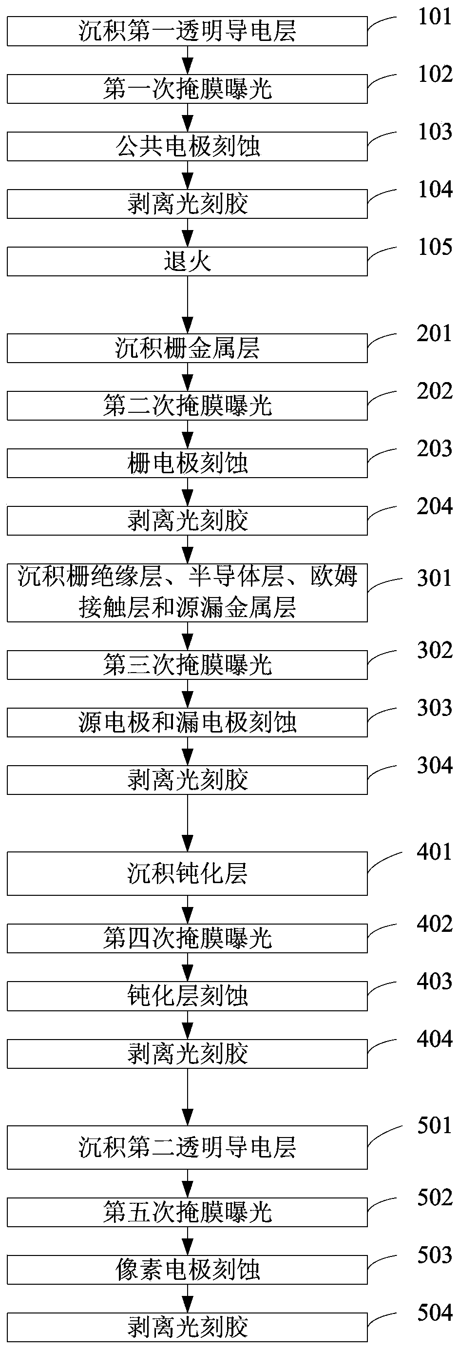
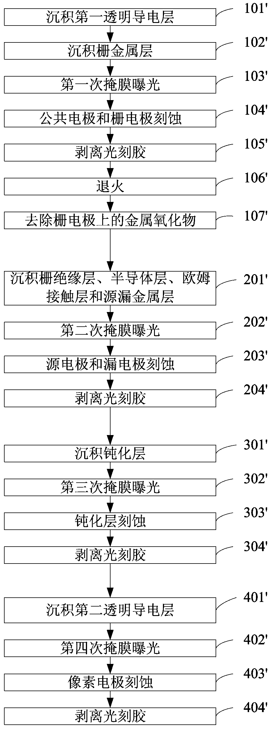
[0047] The embodiments of the present invention aim at the metal electrode formed on the surface of the metal electrode caused by the metal oxide formed on the surface of the metal electrode in the prior art, which causes the impedance of the metal electrode to increase and the electrical conductivity to decrease; and also makes the surface of the metal electrode relatively rough, so that The insulating layer covered on the metal electrode falls off, and a short circuit occurs, seriously affecting the performance of the TFT, resulting in the problem that the display cannot be displayed normally. An array substrate and its manufacturing method and display device are provided, which can remove the metal oxide on the surface of the metal la...
PUM
 Abstract
Description
Claims
Application Information