LED epitaxial wafer

A technology of LED epitaxial wafer and contact layer, which is applied in the direction of electrical components, circuits, semiconductor devices, etc., and can solve the problems of large voltage drop and affecting the luminous effect

Inactive Publication Date: 2013-12-18
SHANDONG KAIYUAN ELECTRONICS
View PDF4 Cites 3 Cited by
  • Summary
  • Abstract
  • Description
  • Claims
  • Application Information

AI Technical Summary

Problems solved by technology

It is difficult to achieve the purpose of reducing the cost of chip production by reducing the chip size by using the existing LED epitaxial wafers
There are also LED epitaxial wafers with two multi-quantum well light-emitting layers, the two multi-quantum well light-emitting layers are connected in series, and the connection layer in the middle produces a large voltage drop and affects the luminous effect.

Method used


Image

  • LED epitaxial wafer
  • LED epitaxial wafer

Examples


Embodiment Construction

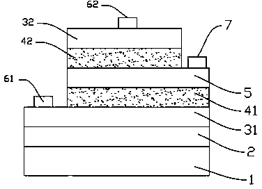
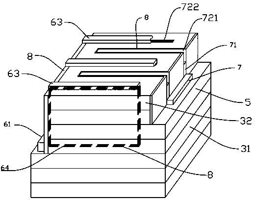
[0015] Depend on figure 1 As shown, the LED epitaxial wafer includes a sapphire substrate 1, a GaN buffer layer 2, a first N-GaN contact layer 31, a first multi-quantum well light-emitting layer 41, a P-GaN contact layer 5, The second multi-quantum well light emitting layer 42 and the second N-GaN contact layer 32 . A P-type electrode 7 electrically connected to the P-GaN contact layer 5 is provided, and an N-type electrode (61, 62) is respectively provided on the first N-GaN contact layer 31 and the second N-GaN contact layer 32, The two N-type electrodes can be set separately and connected in parallel before packaging, or they can be connected first and then packaged. Both quantum well light-emitting layers are InGaN / GaN blue multi-quantum layers. The double multi-quantum light-emitting layer arranged in parallel, compared with the chip arranged on one side, doubles the light-emitting area, reduces the forward voltage drop, improves the uniformity of the current in the int...


PUM


Abstract

The invention discloses an LED epitaxial wafer. The LED epitaxial wafer comprises a substrate, a GaN buffer layer, a first N-GaN contact layer, a first multiple quantum well luminous layer, a P-GaN contact layer, N-type electrodes and a P-type electrode, wherein the substrate, the GaN buffer layer, the first N-GaN contact layer, the first multiple quantum well luminous layer, the P-GaN contact layer, the N-type electrodes and the P-type electrode are stacked in sequence, a second multiple quantum well luminous layer and a second N-GaN contact layer are arranged on the other face of the P-GaN contact layer in sequence, and the first N-GaN contact layer and the second N-GaN contact layer are connected with the N-type electrodes. According to the LED epitaxial wafer, due to the fact that the luminous layers which are connected in parallel are arranged on the two sides of the P-GaN contact layer, the area of the active luminous layers is doubled, the density of current flowing through the luminous layers is reduced by 50% under the condition of the same drive current, the degree of uniformity of the density of the current is improved, the frequency of the phenomenon that the current restrains recession is reduced, the forward voltage drop of an LED is reduced, and the luminous efficiency of the LED is high. Due to the fact that the area of the luminous layers is increased, the area of a chip can be reduced under the condition that the luminance is ensured, the drive current is improved, the cost of the LED chip can be reduced, and luminous efficiency cannot be reduced.

Description

technical field [0001] The invention belongs to the technical field of LED lighting, and in particular relates to an LED epitaxial wafer. Background technique [0002] In the production of existing LEDs, the cost of LED chips accounts for more than half of the overall cost; reducing the size of blue LED chips, thereby reducing the overall production cost of LEDs, is currently a common approach adopted by most manufacturers. After the size of the LED chip is reduced, in order to keep the brightness unchanged, it is necessary to increase the current density input to the LED chip. However, there is a phenomenon of current suppression decline in LEDs, that is, the higher the current density, the lower the luminous efficiency of the LED chip, and the higher the current density, the greater the energy loss. Therefore, simply reducing the chip size is not the fundamental way to reduce the cost of LED chips. [0003] In order to weaken the problem of LED current suppression fading...

Claims


Application Information

Patent Timeline
Patent Type & Authority Applications(China)
IPC IPC(8): H01L33/06H01L33/02
Inventor 刘树高安建春
Owner SHANDONG KAIYUAN ELECTRONICS
Why Eureka
Try Eureka