Transparent electric conduction film

A technology of transparent conductive film and conductive layer, which is applied to conductive layers on insulating carriers, electrical digital data processing, instruments, etc. Electricity increase and other issues, to achieve the effect of low power consumption, smaller impedance, and less stimulation

Inactive Publication Date: 2013-12-25
苏州胜利光学玻璃有限公司
View PDF7 Cites 11 Cited by
  • Summary
  • Abstract
  • Description
  • Claims
  • Application Information

AI Technical Summary

Problems solved by technology

However, the ITO material is expensive and the production cost is high; and limited by the coating temperature, ITO plating on the substrate cannot achieve low impedance, which is not conducive to making a large-area touch screen. High impedance capacitive touch screens will reduce performance and even drive IC will not be able to drive its normal operation
[0004] In addition, the light transmittance of the conductive film made of ITO is not very high, usually only about 80%-88%, which affects the brightness, contrast and color of the display Wait, when the light transmittance is low, if you want to see the screen clearly, you must increase the brightness, the power consumption of the device will inevitably increase, and the irritation to the eyes will also increase

Method used


Image

  • Transparent electric conduction film
  • Transparent electric conduction film

Examples


Embodiment 1

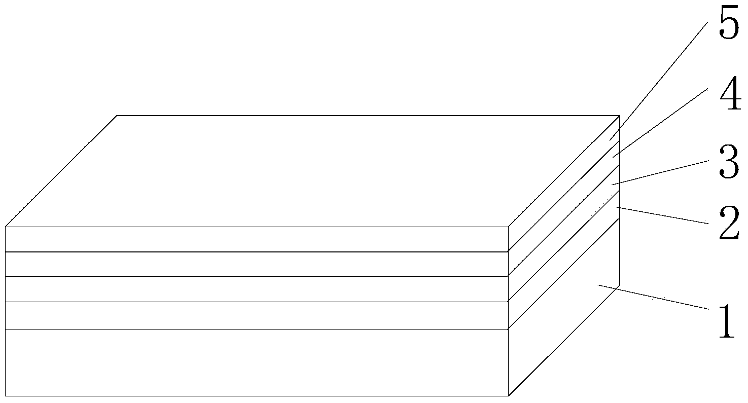
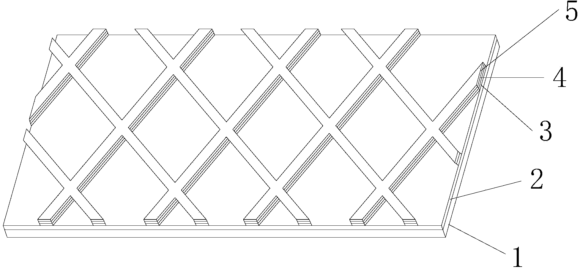
[0027] Embodiment 1 of the present invention provides a transparent conductive film, such as figure 1 As shown, the transparent conductive film involved in the present invention includes a substrate 1, a bottom layer 2, a black layer 3, a conductive layer 4, and a protective layer 5 from bottom to top. The first surface and the second surface of the base material 1 are first coated with the bottom layer 2 by vacuum sputtering or evaporation coating on the second surface of the substrate 1. The bottom layer 2 is a transparent SiO2 layer, and ink can be sprayed on the second surface to form ink pattern; then on the bottom layer 2, a black layer 3, a conductive layer 4 and a protective layer 5 are sequentially plated, wherein the black layer 3 is a mixture of chromium oxide and nickel oxide, and its thickness is 40nm-100nm, and the method of optical interference can be used to Make the black surface visible to the naked eye; the conductive layer 4 is a metal layer, preferably ...

Embodiment 2

[0029] Embodiment 2 of the present invention provides another kind of transparent conductive film, and present embodiment compares with embodiment 1, and protective layer 5 is changed into black layer 3, and black layer 3 can also play the function of preventing oxidation, like this, naked eyes also can Ability to observe from the other side.


PUM

PropertyMeasurementUnit
thicknessaaaaaaaaaa
thicknessaaaaaaaaaa
transmittivityaaaaaaaaaa

Abstract

The invention discloses a transparent electric conduction film which comprises a base material. A plating bottom layer, a black layer, an electric conduction layer and a protective layer are sequentially arranged on the surface of the base material. Pattern etching is performed on the black layer, the electric conducting layer and the protection layer, and grid line patterns are formed. Grid lines are distributed in the first direction and in the second direction. Grid units formed between every two adjacent grid lines are transparent areas, and the transparent areas are in quadrangle shapes. The electric conduction layer is a metal grid, impedance is low, and the transparent electric conduction film is suitable for middle-screen touch screens and large-screen touch screens. In addition, the transparent electric conduction film has high transmittance and the high anti-interference capacity and reduces power consumption of equipment. Compared with an ITO electric conduction film in the prior art, the metal grid greatly reduces cost.

Description

technical field [0001] The invention relates to the technical field of conductive layers, in particular to a transparent conductive film of a metal grid. Background technique [0002] Transparent conductive films are widely used in touch screens, flat panel displays, photovoltaic devices, electromagnetic shielding and other fields, especially in the field of capacitive touch screens. A touch screen is a sensing device that can receive input signals such as touch. The touch screen has endowed information interaction with a new look and is a very attractive new information interaction device. The development of touch screen technology has attracted widespread attention at home and abroad, and has become a rising high-tech industry in the optoelectronic industry. [0003] The transparent conductive film is a crucial component of the touch screen. At present, the conductive film of the touch screen is mainly formed on an insulating substrate by vacuum coating and pattern etchi...

Claims


Application Information

Patent Timeline
Patent Type & Authority Applications(China)
IPC IPC(8): H01B5/14G06F3/044
Inventor 王立新
Owner 苏州胜利光学玻璃有限公司
Why Eureka
Try Eureka