Array substrate and manufacturing method thereof

A technology of an array substrate and a manufacturing method, which is applied in the display field, can solve the problems of widening the width of the wiring area, reducing the number of signal lines, and increasing the number of drivers, and achieves the effects of extending the length, reducing the manufacturing cost, and increasing the length and resistance of the signal lines Effect

Inactive Publication Date: 2013-12-25
BOE TECH GRP CO LTD +1
View PDF7 Cites 28 Cited by
  • Summary
  • Abstract
  • Description
  • Claims
  • Application Information

AI Technical Summary

Problems solved by technology

In order to make the signal line 011 and the signal line 012 form an equal-resistance conduction path, the signal line 012 is made into a zigzag shape, but the formation of the zigzag line will cause the width of the wiring area occupied by the signal line to widen
In the prior art, when folded lines are formed on the same layer of the array substrate, the width occupied by the signal line 012 is d, so that the number of signal lines that can be accommodated in the same area of ​​the wiring area is reduced, which in turn leads to an increase in the number of drivers (COF, etc.) , the increase in the number of drivers will inevitably lead to an increase in the number of driver ICs, which ultimately leads to an increase in cost

Method used


Image

  • Array substrate and manufacturing method thereof
  • Array substrate and manufacturing method thereof
  • Array substrate and manufacturing method thereof

Examples


Embodiment 1

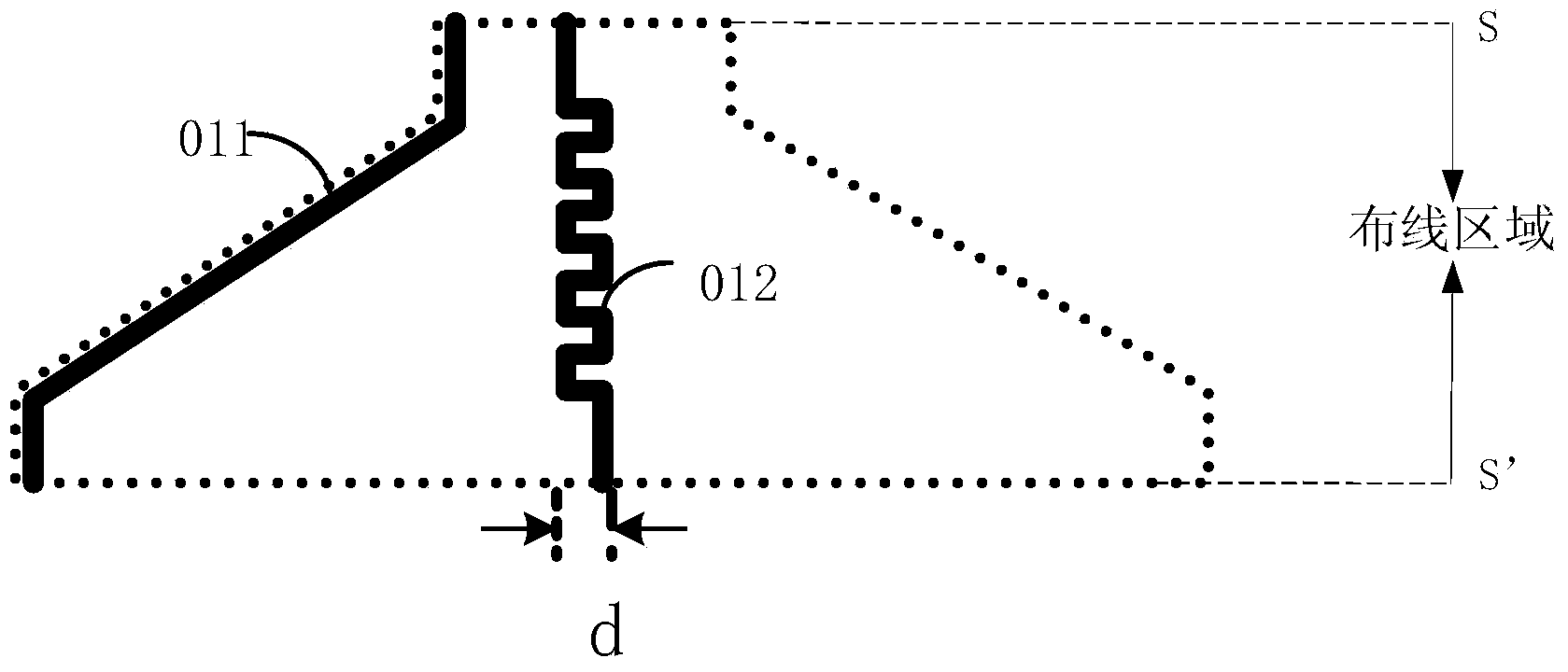
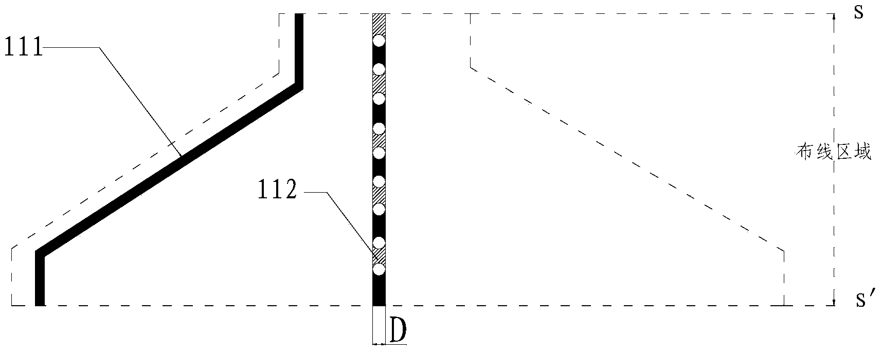
[0075] The array substrate of this embodiment includes a plurality of wiring areas arranged in the non-display area, and several signal lines are arranged in the wiring areas, and at least part of the signal lines in each wiring area are connected in series by wires located in different layers. formed; the resistance difference between any two signal lines in the same wiring area is within the threshold range.

[0076] The array substrate is divided into a display area located in the middle, which is usually also referred to as an AA area, and a non-display area located at the periphery of the display area. Usually, after the array substrate is assembled into a display device, the non-display area is covered by a frame of the display device. There are multiple wiring areas in the non-display area; several signal lines are arranged in each of the wiring areas; the signal lines can be gate lines or data lines; the signal lines are located in the part of the wiring area It is us...

Embodiment 2

[0094] The array substrate of this embodiment includes a plurality of wiring areas arranged in the non-display area, and several signal lines are arranged in the wiring areas, and at least part of the signal lines in each wiring area are connected in series by wires located in different layers. formed; the resistance difference between any two signal lines in the same wiring area is within the threshold range. The wires of different layers are sequentially connected according to the extending direction of the signal wires.

[0095] specific as Figure 6 As shown, the array substrate includes a pixel electrode layer, a gate line metal layer, and a source-drain metal layer. specific as Figure 6 The middle signal line is located in the non-display area of ​​the array substrate, including signal line 210, signal line 220, and signal line 230. If traditional single-layer wiring is used, since the signal line 210 is located at the outermost periphery of the connecting wiring area...

Embodiment 3

[0103] This embodiment provides a manufacturing method of an array substrate, the manufacturing method comprising: forming a signal line located in a non-display area and connected to a gate line or a data line, and the signal line is formed by connecting wires located in different layers in series; Wherein, the signal lines are located in the wiring area of ​​the non-display area of ​​the array substrate; and the resistance difference between any two signal lines in the same wiring area is within a threshold range.

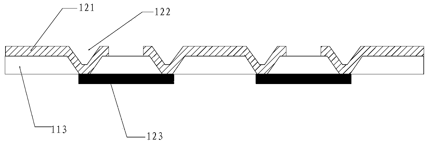
[0104] Specifically, wires located in different layers to form signal wires include at least the following two structures:

[0105] In the first type, in at least one conductive layer used to form wires in the array substrate, several wires are formed, and the wires located in different layers are correspondingly connected in series.

[0106] The second type is to form a wire corresponding to a signal line in the conductive layer used to form wires on the array s...


PUM


Abstract

The invention discloses an array substrate and a manufacturing method thereof. The problems that signal lines in an existing array substrate are all placed on the same layer, so that equal resistance between the signal lines is achieved, part of the signal lines are horizontally bent, and accordingly signal line density of a wiring zone is small, the drive number is large, and cost is high are solved. The array substrate comprises a plurality of wiring zones arranged on a non-displaying zone, a plurality of signal lines are arranged in the wiring zones, at least part of the signal lines in each wiring zone are formed by leading wires in different layers in a series-connecting mode, and the resistance difference between any two signal lines in the same wiring zone is in the threshold value range. According to the array substrate and the manufacturing method thereof, traditional signal lines placed in one layer of the array substrate are changed to the signal lines placed between the multiple layers, so that the fact that the resistance difference between the signal lines is smaller than the threshold value and the bending radius of the signal lines is small is facilitated, signal line concentrating density is large, the drive number is lowered, and the purpose of cost lowering is achieved.

Description

technical field [0001] The present invention relates to the display field, in particular to an array substrate and a manufacturing method thereof. Background technique [0002] Structures such as gate lines, data lines, thin film transistors, and pixel electrodes are arranged on the array substrate; the above structures are all made of different layers of conductive materials. Generally, the array substrate has a layered structure including a gate metal layer forming a gate, a source-drain metal layer forming a source and drain of a thin film transistor, and a pixel electrode layer forming a pixel electrode. Some array substrates also include a common electrode layer forming a common electrode. Wherein, the gate line is connected to the gate of the thin film transistor; the data line is connected to the source of the thin film transistor; the gate line is used to turn on the thin film transistor, and the data line is used to input a voltage signal to the pixel electrode thr...

Claims


Application Information

Patent Timeline
Patent Type & Authority Applications(China)
IPC IPC(8): H01L27/12H01L21/77
CPCG02F1/1345H01L27/124H01L27/1248H01L27/1259
Inventor 张明樊超崔立全郝昭慧尹雄宣
Owner BOE TECH GRP CO LTD
Why Eureka
Try Eureka