Packaging method and structure of chip embedded in substrate

A packaging method and packaging structure technology, which is applied in the fields of electrical components, electrical solid devices, semiconductor/solid device manufacturing, etc., can solve the problems of bare chip integrity risk and great pressure, and achieve good scalability and strong applicability Effect

Active Publication Date: 2017-02-01
SHENNAN CIRCUITS
View PDF3 Cites 3 Cited by
  • Summary
  • Abstract
  • Description
  • Claims
  • Application Information

AI Technical Summary

Problems solved by technology

[0004] Embed semiconductor chips of different thicknesses into the substrate. Due to the need for insulation, when the thickness of the substrate is required to be different from that of the bare chip, due to the needs of screen printing and other processes, it is necessary to ensure that at least one side of the chip is coplanar with the substrate, and at the same time ens...

Method used


Image

  • Packaging method and structure of chip embedded in substrate
  • Packaging method and structure of chip embedded in substrate
  • Packaging method and structure of chip embedded in substrate

Examples


Embodiment 1

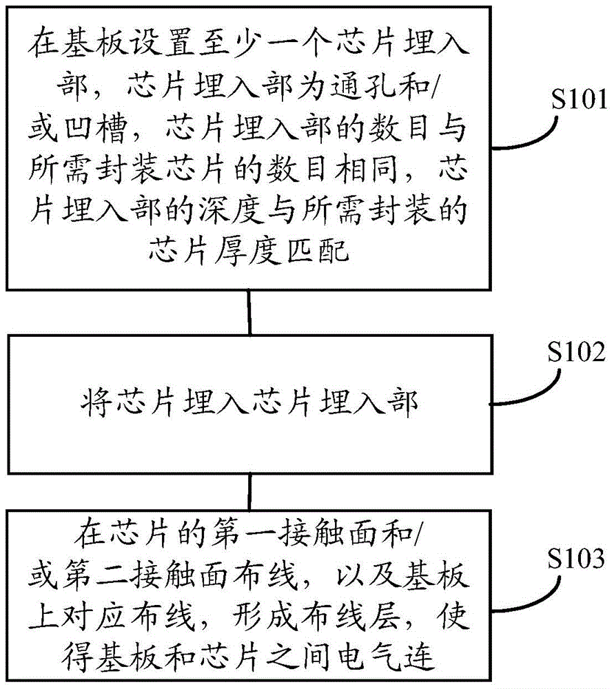
[0030] refer to figure 1 , which is a schematic flow chart of a method for packaging a chip embedded in a substrate in this embodiment, a method for packaging a chip embedded in a substrate, wherein the chip has a first contact surface and a second contact surface, comprising the following steps:

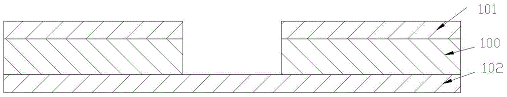
[0031] S101, setting at least one chip embedding part on the substrate, the chip embedding part is a through hole and / or groove, the number of chip embedding parts is the same as the number of chips to be packaged, and the depth of the chip embedding part matches the thickness of the chip to be packaged ;

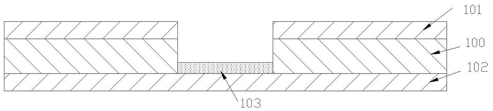
[0032] S102, embedding the chip into the chip embedding part;

[0033] S103, wiring on the first contact surface and / or the second contact surface of the chip, and corresponding wiring on the substrate, forming a wiring layer, so that the substrate and the chip are electrically connected.

[0034] As for the chip embedding part being a through hole and / or a groove, in different...

Embodiment 2

[0089] refer to Figure 6 , which is a schematic flow chart of another embodiment of a packaging method for embedding a chip into a substrate, the chip has a first contact surface and a second contact surface, and includes the following steps:

[0090] S601, opening at least one through hole on the substrate, the number of through holes is the same as the number of chips to be packaged, and the through hole penetrates through the substrate;

[0091] Wherein, the substrate can be a single-sided board, a double-sided board or a multi-layer board.

[0092] S602, taking the thick copper foil and etching out the protrusions that are consistent with the distribution of the positions of the through holes;

[0093] S603, the substrate and the thick copper foil are laminated and connected through the insulating medium layer, the through hole and the convex part form a groove, and the depth of the groove matches the thickness of the chip to be embedded. When the substrate needs to be b...

Embodiment 3

[0107] Figure 8 Shown is a schematic flow chart of another embodiment of a packaging method for embedding a chip into a substrate, the chip has a first contact surface and a second contact surface, and includes the following steps:

[0108] S801, opening at least one through hole on the substrate, the number of through holes is the same as the number of chips to be packaged;

[0109] S802, coating a layer of photosensitive material on the surface of the second metal layer to form a photosensitive material layer;

[0110] S803, connecting the second contact surface of the chip with the photosensitive material layer, so that the chip is buried in the through hole;

[0111] S804, filling the gap between the chip and the through hole with an adhesive material for fixing the chip;

[0112] S805, removing the photosensitive material layer;

[0113] S806, printing conductive paste on the first contact surface;

[0114] S807, disposing wiring on the first contact surface and / or t...


PUM


Abstract

Provided are an encapsulation method for embedding a chip into a substrate and a structure thereof. The method includes: providing at least one chip embedding part inside a substrate, the chip embedding part being a through-hole and/or a recess, the number of chip embedding parts being equal to that of the chip (107) to be encapsulated, the depth of the chip embedding part matched with the thickness of the chip (107) to be encapsulated; embedding the chip (107) into the chip embedding part; wiring on a first contact face and/or a second contact face of the chip (107), and wiring correspondingly on the substrate to form a wiring layer, so that the substrate and the chip (107) are electrically connected to each other.

Description

technical field [0001] The invention relates to the field of chip packaging, in particular to a packaging method and structure of a chip embedded in a substrate. Background technique [0002] With the development of the information society, the amount of information processed by various electronic devices is increasing, and the demand for high-frequency and high-speed signal transmission is increasing. Embedding the semiconductor chip into the packaging substrate, because it can effectively shorten the connection distance between the semiconductor and the packaging substrate, can provide a strong guarantee for high-frequency and high-speed signal transmission. Miniaturization development needs. [0003] There is a special type of bare chip in semiconductor packaging, such as metal-oxide-semiconductor field-effect transistor (Metal-Oxide-Semiconductor Field-Effect Transistor, MOSFET), diode (diode) and transistors and other active devices, with single-sided or double-sided e...

Claims


Application Information

Patent Timeline
IPC IPC(8): H01L21/50H01L23/48
CPCH01L23/13H01L23/5389H01L24/19H01L2224/04105H01L2224/73267H01L2924/13091H01L2924/15153H01L2924/00
Inventor 霍如肖谷新丁鲲鹏
Owner SHENNAN CIRCUITS
Why Eureka
Try Eureka