
Small-size led packaging structure for enhancing light emitting angle

A technology of light-emitting diodes and improved structures, applied in electrical components, electric solid-state devices, circuits, etc., can solve the problems of reduced LED applicability, poor molding, and difficulty in subsequent use, and achieves reduction of packaging process costs, color performance, and color performance. The effect of improving usability

Inactive Publication Date: 2014-01-01
UNITY OPTO TECH CO LTD
View PDF4 Cites 49 Cited by
  • Summary
  • Abstract
  • Description
  • Claims
  • Application Information

AI Technical Summary

Problems solved by technology

For example, if the sidewalls are kept as far away from the light-emitting chip as possible, the sidewalls are less likely to block the side light emitted by the light-emitting chip and can form a wider light-emitting angle, but at this time, the LED will have a package structure with a certain volume. It does not conform to the trend of miniaturization of electronic products and is not easy to follow-up application, which reduces the applicability of LED in various fields
In addition, if the height of the side wall is simply reduced, the colloid will not be easily solidified and the shape will be poor, which will affect the luminous efficiency of the LED.
[0004] It can be seen that no matter which method is used above, the maximum luminous angle of the existing LED is still only about 120°, which limits its lighting range and radiation angle in subsequent applications.

Method used


Image

  • Small-size led packaging structure for enhancing light emitting angle
  • Small-size led packaging structure for enhancing light emitting angle
  • Small-size led packaging structure for enhancing light emitting angle

Examples


Embodiment Construction

[0016] The above and other technical features and advantages of the present invention will be described in more detail below in conjunction with the accompanying drawings.

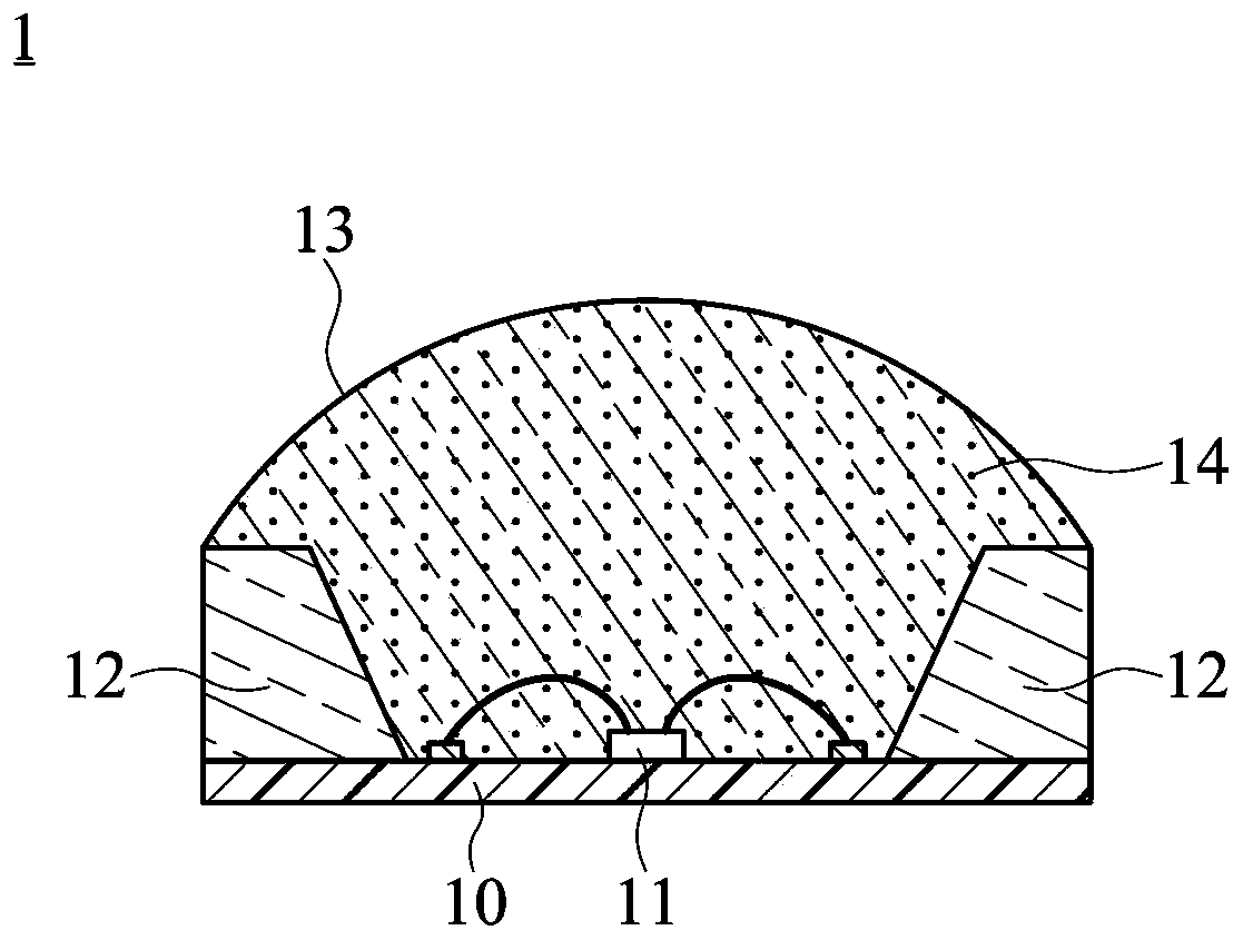
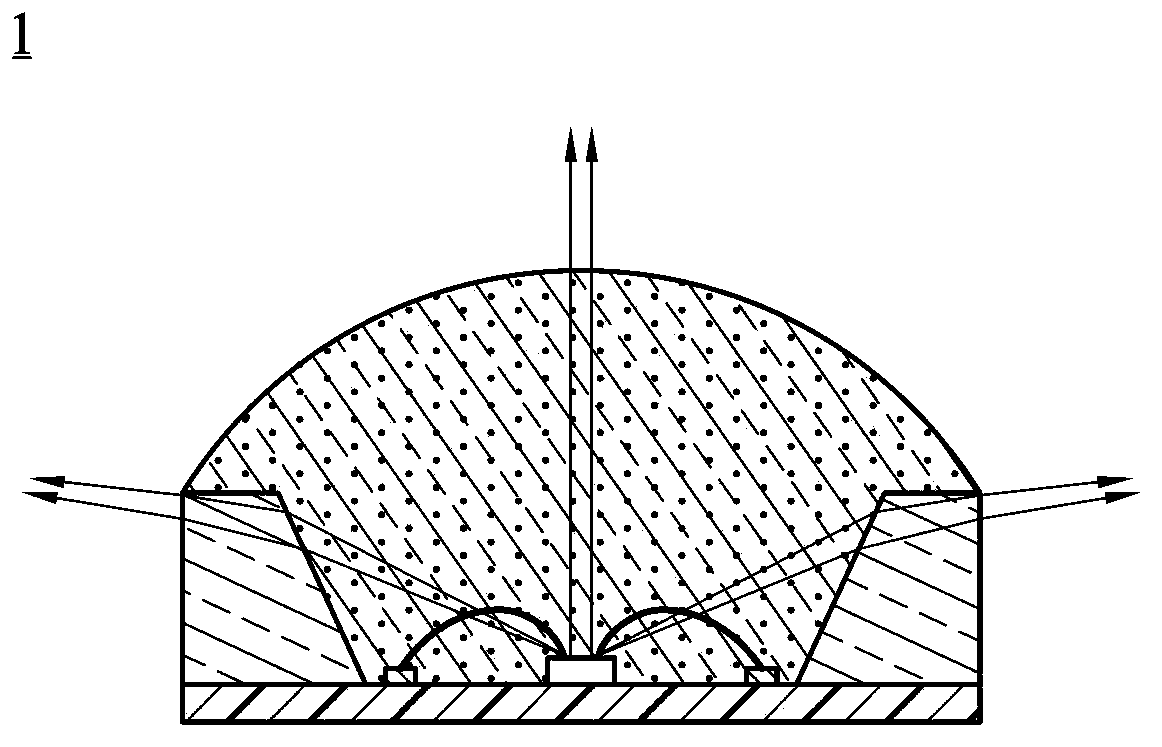
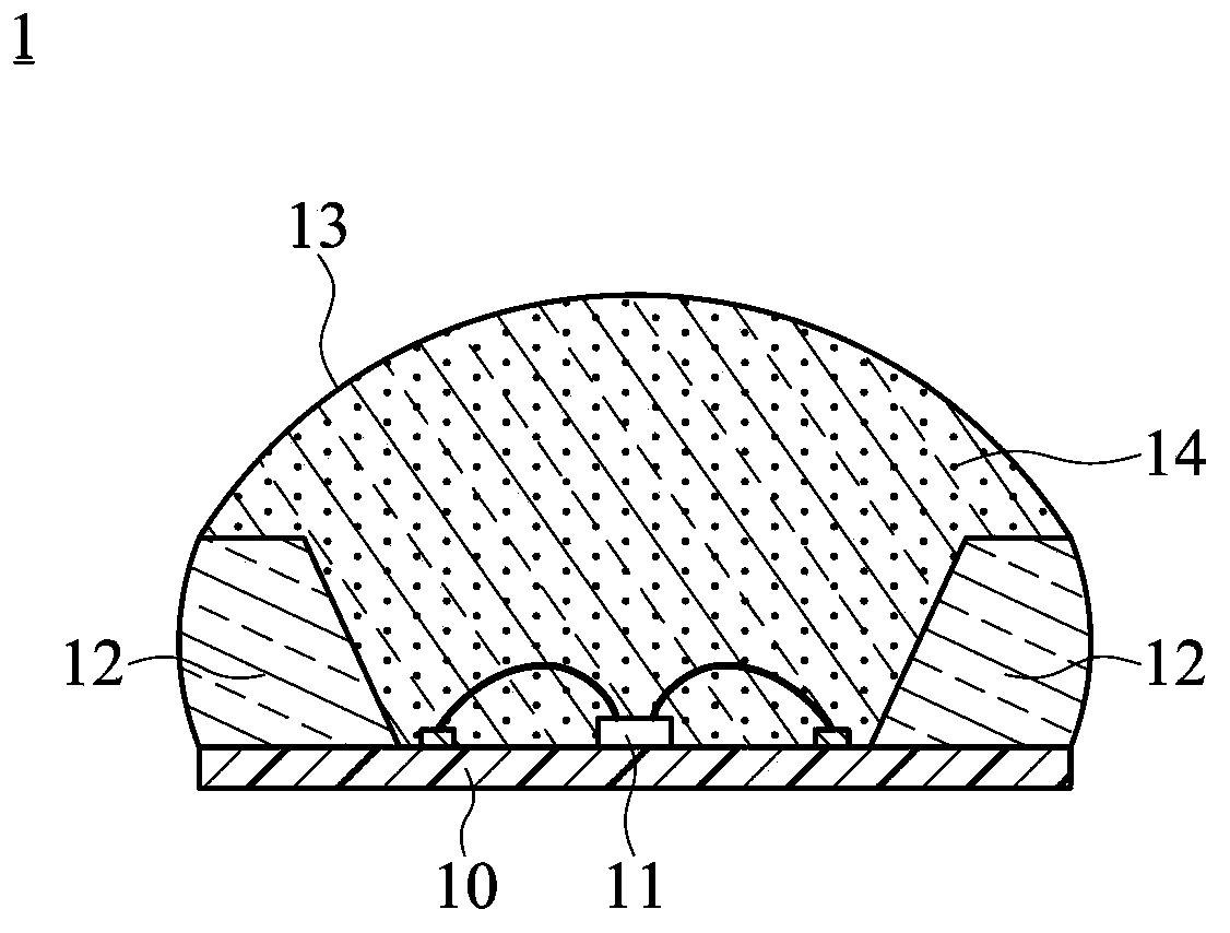
[0017] see figure 1 , figure 2 , are respectively the cross-sectional view and the schematic diagram of the optical path of the first embodiment of the preferred embodiment of the present invention. As shown in the figure, the small-sized light-emitting diode package improvement structure 1 is suitable for lighting devices such as direct-lit backlights or bulb lamps, and has an opaque base 10 and at least one light-emitting chip 11. The light-emitting chip 11 can be yellow light, Red light, blue light or green light LED chips, and the opaque base 10 is surrounded by a transparent side wall 12 to form a concave cup space. The light-emitting chip 11 is disposed on the opaque base 10 and accommodated in the concave cup space, and the light-emitting chip 11 is electrically connected to the positive and nega...


PUM


Abstract

A small-size LED packaging structure for enhancing a Sight emitting angle includes an opaque base and at least one light emitting chip. The light emitting chip is installed on the opaque base, and the opaque base includes a transparent sidewall disposed around the base and a concave-cup space, and the transparent sidewall is formed by a molding method, and the concave-cup space is filled with a packaging gel by a dispensing method, and the packaging gel is doped with at least one phosphor powder. Therefore, the transparent sidewall can increase the light emitting angle to 140°~180° and reduce the amount of internal reflected light significantly to avoid the occurrence of a yellow ring phenomenon, and the phosphor powder can enhance the color manifestation and the color gamut.

Description

technical field [0001] The invention relates to the technical field of light-emitting diode packaging structures, in particular to an improved small-sized light-emitting diode packaging structure that improves the light-emitting angle. Background technique [0002] Existing light-emitting diodes (Light-Emitting Diodes, LEDs) are mainly manufactured by carrying a light-emitting chip on a flat substrate or a concave cup-shaped substrate, and are manufactured after wire bonding and sealing. Among them, although the LED packaging structure using a flat substrate has a wider light-emitting angle, the flat substrate cannot be directly dispensed with glue, and the subsequent assembly process is more complicated, resulting in high manufacturing costs, which is not economical. Furthermore, the colloid is a thick semi-fluid object, which is difficult to form in a fixed area. Therefore, LEDs often have a poor optical luminous effect due to poor colloid formation, which in turn affects ...

Claims


Application Information

Patent Timeline
Patent Type & Authority Applications(China)
IPC IPC(8): H01L33/48H01L33/54H01L33/58
CPCH01L33/58H01L33/50H01L33/54H01L2224/48091H01L2924/181H01L2924/00012H01L2924/00014
Inventor 林威冲吴秉宸
Owner UNITY OPTO TECH CO LTD
Learn More