White light led packaging process

A technology of LED packaging and white light, which is applied in the direction of electrical components, circuits, semiconductor devices, etc., can solve the problems that affect LED luminous efficiency and cannot improve color uniformity, achieve improved LED color uniformity, good spatial color uniformity, and overcome The effect of settlement

Inactive Publication Date: 2016-11-23
成都天星永光照明电器有限公司
View PDF4 Cites 4 Cited by
  • Summary
  • Abstract
  • Description
  • Claims
  • Application Information

AI Technical Summary

Problems solved by technology

In the prior art, in order to solve the problem of phosphor sedimentation, those skilled in the art generally consider methods such as phosphor sedimentation and centrifugation to improve the color uniformity of LEDs, but these methods require precise control of the speed of sedimentation and centrifugation And time problems, if the control is not good, not only can not improve the color uniformity, but also may affect the luminous efficiency of LED

Method used


Image

  • White light led packaging process
  • White light led packaging process
  • White light led packaging process

Examples


Embodiment 1

[0025] A white light LED packaging process, comprising the following steps:

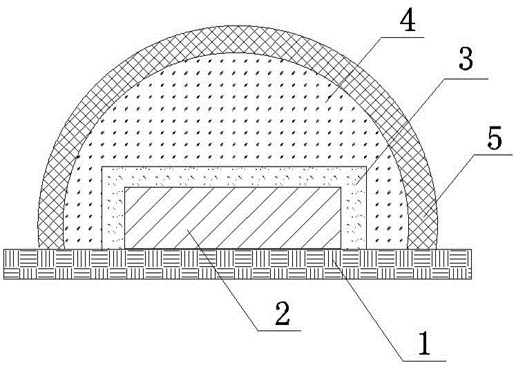
[0026] (a) Die-bonding and wire-bonding the blue LED chip 2 on the substrate 1;

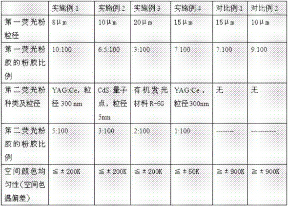
[0027] (b) Preparation of the first fluorescent powder glue: Select the commercial yellow phosphor YAG-04 with a particle size of 8 μm and mix it in Shin-Etsu 5547 silica gel, the ratio of phosphor to glue is 10:100, stir and degas to obtain the first phosphor glue;

[0028] (c) Forming the first phosphor layer 3 on the LED wafer 2 with the first phosphor glue by a conformal coating method;

[0029] (d) putting the LED chip 2 coated with the first phosphor layer 3 into an oven for solidification, and taking it out after cooling to room temperature;

[0030] (e) Prepare the second phosphor glue: mix YAG:Ce inorganic phosphor with a particle size of 300nm in Dow Corning 6650 silica gel, control the ratio of YAG:Ce phosphor to Dow Corning 6650 silica gel at 5:100, stir and degas , to obtain the second phosphor glue;

...

Embodiment 2

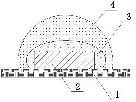
[0035] A white light LED packaging process, comprising the following steps:

[0036] (a) Die-bonding and wire-bonding the blue LED chip 2 on the substrate 1;

[0037](b) Preparation of the first phosphor glue: mix commercial yellow phosphor YAG-04 with a particle size of 10 μm and orange phosphor O5742 (the ratio of yellow phosphor YAG-04 to orange phosphor O5742 is 7:3) in Shin-Etsu 5547 In silica gel, the ratio of phosphor to glue is 6.5:100, stir and degas to obtain the first phosphor glue;

[0038] (c) Forming the first phosphor layer 3 on the LED wafer 2 with the first phosphor glue by a dispensing coating method;

[0039] (d) putting the LED chip 2 coated with the first phosphor layer 3 into an oven for solidification, and taking it out after cooling to room temperature;

[0040] (e) Prepare the second phosphor glue: mix CdS quantum dots with a particle size of 5nm in Dow Corning 6650 silica gel, control the ratio of phosphor to glue at 3:100, stir and degas to obtain ...

Embodiment 3

[0045] A white light LED packaging process, comprising the following steps:

[0046] (a) Die-bonding and wire-bonding the blue LED chip on the substrate;

[0047] (b) Preparation of the first phosphor glue: Mix commercial yellow phosphor YAG-04 with a particle size of 20 μm and nitride red phosphor (the ratio of yellow phosphor YAG-04 to nitride red phosphor is 6:4) in In the epoxy glue, the ratio of phosphor to glue is 3:100, mix, stir, and degas to obtain the first phosphor glue;

[0048] (c) Forming the first phosphor layer 3 on the LED wafer 2 with the first phosphor glue by a dispensing coating method;

[0049] (d) putting the LED wafer 2 coated with the first phosphor layer 3 into an oven for curing, the baking time is 1-3 hours, the baking temperature is 100-150 degrees Celsius, and taken out after cooling to room temperature;

[0050] (e) Prepare the second fluorescent powder glue: dissolve the organic light-emitting material R-6G in the second colloid--molding glue,...


PUM

PropertyMeasurementUnit
particle diameteraaaaaaaaaa

Abstract

The invention discloses white light LED packing process. The white light LED packing process comprises the steps of forming a first fluorescent powder layer (3) on an LED wafer (2) and forming a second fluorescent powder layer (4). The step of forming the second fluorescent powder layer is that second fluorescent powder gum is moulded and sealed on the first fluorescent powder layer (3). The second fluorescent powder gum comprises second fluorescent powder and second colloid, wherein the particle size of the second fluorescent powder is smaller than 1 mum, the second fluorescent powder is one kind or several kinds of inorganic fluorescent powder, quantum dots and an organic light-emitting material, and the mass proportion between the second fluorescent powder and the second collide is not higher than 5:100. The two kinds of the fluorescent powder with different particle sizes are matched to be used, so that the sufficient brightness of an LED is guaranteed, the sedimentation problem of the fluorescent powder is solved, the color uniformity of the LED can be improved by adjusting absorption of blue light, and a white light LED with good spatial color uniformity is achieved.

Description

technical field [0001] The invention relates to an LED encapsulation process, in particular to a white LED encapsulation process. Background technique [0002] Light-emitting diode (LED) is a semiconductor light source. Compared with other light sources such as incandescent lamps, LEDs have many advantages. LEDs usually have longer life, better stability, faster switching characteristics, and lower energy consumption. As the LED as a new generation of light source has become more and more popular in people's lives, its application has become more and more extensive. In terms of synthesizing white light, the most common way is to place a wavelength conversion material, such as yellow phosphor, on a blue-emitting LED chip. The layer of wavelength conversion material on the LED chip will absorb some of the photons emitted by the LED and convert them down. (down-convert) to visible wavelengths of light, resulting in a two-color light source with blue and yellow wavelengths of l...

Claims


Application Information

Patent Timeline
Patent Type & Authority Patents(China)
IPC IPC(8): H01L33/50
CPCH01L33/504H01L33/505H01L33/507H01L2933/0041H01L2933/005
Inventor 马文波王建全梁丽陈可
Owner 成都天星永光照明电器有限公司
Why Eureka
Try Eureka