Single-phase high-gain boost converter

A boost converter, high-gain technology, applied in the direction of conversion equipment without intermediate conversion to AC, can solve the problems of difficult to meet high-gain conversion requirements, large switch current peak impact, large input current ripple, etc. Achieve the effect of facilitating input current filtering, small input current ripple, and realizing voltage gain

Active Publication Date: 2014-01-01
SOUTH CHINA UNIV OF TECH
3 Cites 17 Cited by

AI-Extracted Technical Summary

Problems solved by technology

[0003] At present, the most commonly used boost converter is a single-tube Boost converter. However, the boost range of this converter is very limited. Usually, the boost multiple is within ten times, and it is difficult to meet the high-gain conversion requirements.
Based on the conventional single-transistor Boost converter, the coupled inductor technology can achieve gain expansion, but the input ...

Method used

[0068] The present invention utilizes two capacitors, ie, the second capacitor C2 and the third capacitor C3, to realize voltage transfer, w...

Abstract

The invention provides a single-phase high-gain boost converter. The single-phase high-gain boost converter mainly comprises a voltage transfer circuit, a coupling inductance booster circuit and an output circuit, wherein the voltage transfer circuit, the coupling inductance booster circuit and the output circuit are connected in sequence. The voltage transfer circuit comprises a first inductor, a switching tube and a first capacitor. The coupling inductance booster circuit comprises a primary winding and a secondary winding which are coupled with the inductor, a second capacitor, a third capacitor, a first diode and a second diode. The output circuit comprises a third diode, a fourth capacitor and a load. The single-phase high-gain boost converter is simple in structure and high in output voltage gain.

Application Domain

Technology Topic

Image

  • Single-phase high-gain boost converter
  • Single-phase high-gain boost converter
  • Single-phase high-gain boost converter

Examples

  • Experimental program(1)

Example Embodiment

[0028] Example
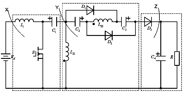
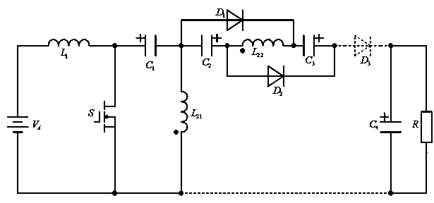
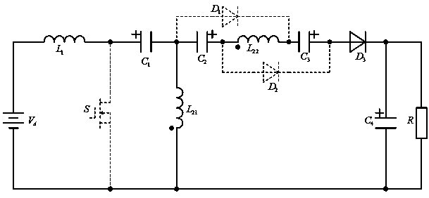
[0029] Such as figure 1 As shown, a single-phase high-gain boost converter includes a voltage transfer circuit X, a coupled inductor boost circuit Y, and an output circuit Z that are connected in sequence.
[0030] The voltage transfer circuit X includes a first inductor L 1 , The switch tube S and the first capacitor C 1;
[0031] The coupled inductor boost circuit Y includes a primary winding L of the coupled inductor 21 And the secondary winding L of the coupled inductor 22 , The second capacitor C 2 , The third capacitor C 3 , The first diode D 1 And the second diode D 2;
[0032] The output circuit includes a third diode D 3 , The fourth capacitor C 4 And load R.
[0033] The first inductor L 1 And the input power V g The positive connection, the first inductor L 1 The other end of the switch tube S and the first capacitor C 1 One end connected;
[0034] The source of the switch S and the input power V g The negative connection;
[0035] The first capacitor C 1 The other end is connected to the first diode D 1 Anode, second capacitor C 2 One end of the coupled inductor primary winding L 21 The synonymous end connection;
[0036] The primary winding L of the coupled inductor 21 The end of the same name and the input power V g The negative connection;
[0037] The first diode D 1 And the third capacitor C 3 One end of the coupled inductor secondary winding L 22 The synonymous end connection;
[0038] The second capacitor C 2 The other end of the coupled inductor is connected to the secondary winding L 22 The second diode of the same name end D 2 The anode connection;
[0039] The third capacitor C 3 The other end is connected to the second diode D 2 The cathode, the third diode D 3 The anode connection;
[0040] The third diode D 3 And the fourth capacitor C 4 Connect one end of the load R to one end;
[0041] The fourth capacitor C 4 The other end of the load R and the input power V g The negative connection;
[0042] Such as Figure 2a with Figure 2b As shown, a single-phase high-gain boost converter mainly has two operating modes in one switching period, which are described as follows:
[0043] Working mode 1:
[0044] Such as Figure 2a As shown, the switch tube S is turned on, and the first diode D 1 , The second diode D 2 On, the third diode D 3 Deadline. Input power V g Give the first inductor L 1 Charging, the first inductor L 1 Energy storage, the first capacitor C 1 Through the coupled inductor to the second capacitor C 2 , The third capacitor C 3 Transfer energy, the second capacitor C 2 And the third capacitor C 3 Energy storage. The fourth capacitor C 4 Provide energy to load R.
[0045] In this working mode, the relational expressions of related electrical parameters are:
[0046] V L1 =V d (1)
[0047] V L21 =V C1 (2)
[0048] V C2 =V C3 =NV C1 (3)
[0049] Where V d Represents the input power voltage, V L1 Indicates the first inductance L 1 Voltage at both ends of this working mode, V L21 Represents the voltage across both ends of the magnetizing inductance of the coupled inductor in this working mode, V C1 , V C2 , V C3 Respectively represent the first capacitance C 1 , The second capacitor C 2 And the third capacitor C 3 Voltage at both ends, N (N≥1) represents the ratio of the number of turns of the primary winding and the secondary winding of the coupled inductor.
[0050] Working mode 2:
[0051] Such as Figure 2b As shown, the switch S is off, and the third diode D 3 On, the first diode D 1 And the second diode D 2 Deadline. The first inductance L 1 Release energy, the second capacitor and the third capacitor C 3 At the same time release energy to the output circuit, the fourth capacitor C 4 Energy storage.
[0052] In this working mode, the relevant electrical parameter expression is:
[0053] V′ L21 +V C2 +V C3 +NV′ L21 =V o (4)
[0054] V′ L1 +V d =V C2 +V′ L21 (5)
[0055] Where V o Represents the output voltage, V′ L21 Represents the voltage across the magnetizing inductance of the coupled inductor in this working mode, V′ L1 Indicates the first inductance L 1 The voltage across both ends in this working mode.
[0056] Voltage gain analysis when the converter works stably:
[0057] Let the switching period of the switch tube work as T s , The duty cycle is D, that is, the duration of working mode 1 is DT s , The duration of working mode 2 is (1-D)T s. According to the inductance volt-second balance characteristic, we can get:
[0058] V L1 DT s =V′ L1 (1-D)T s (6)
[0059] V L21 DT s =V′ L21 (1-D)T s (7)
[0060] Combining equations (1) to (7) can get:
[0061] V o = 2 N + D - ND 1 - D V d
[0062] It can be derived from this that the voltage gain M of a single-phase high-gain boost converter according to the present invention is:
[0063] M = V o V d = 2 N + D - ND 1 - D
[0064] Compared with the prior art, the present invention has the following advantages:
[0065] The invention does not require an additional power switch, has simple structure, convenient control and high efficiency;
[0066] When the converter of the present invention works, the input current ripple is small, which is convenient for input current filtering;
[0067] The coupled inductor in the present invention participates in energy transfer during the switching on and off of the switch tube, which improves the utilization rate of the coupled inductor;
[0068] The present invention simultaneously uses two capacitors, the second capacitor C 2 And the third capacitor C 3 Realizing the voltage transfer not only realizes the further expansion of the voltage gain, but also further improves the utilization rate of the coupled inductor.

PUM

no PUM

Description & Claims & Application Information

We can also present the details of the Description, Claims and Application information to help users get a comprehensive understanding of the technical details of the patent, such as background art, summary of invention, brief description of drawings, description of embodiments, and other original content. On the other hand, users can also determine the specific scope of protection of the technology through the list of claims; as well as understand the changes in the life cycle of the technology with the presentation of the patent timeline. Login to view more.

Similar technology patents

Classification and recommendation of technical efficacy words

  • Simple structure
  • Easy to control

Beam expanding optical element, beam expansion method, image display apparatus, and head-mounted display

InactiveUS20070188837A1Reduce color unevennessSimple structureOptical light guidesSubstrate with hologramHead worn displayLight wave
Owner:KONICA MINOLTA INC

Microlithographic projection exposure apparatus

InactiveUS20050068499A1Simple structureReliable and low-maintenance operationProjectorsPhotomechanical exposure apparatusCamera lensPhysics
Owner:CARL ZEISS SMT GMBH
Why Eureka
Try Eureka