
Semiconductor wafer and method for manufacturing same

A manufacturing method and semiconductor technology, applied in semiconductor/solid-state device manufacturing, semiconductor devices, manufacturing tools, etc., to achieve the effect of improving productivity and yield

Active Publication Date: 2014-01-01
SHIN-ETSU HANDOTAI CO LTD
View PDF6 Cites 3 Cited by
  • Summary
  • Abstract
  • Description
  • Claims
  • Application Information

AI Technical Summary

Problems solved by technology

Also, the thickness of the semiconductor wafer varies greatly between 0.5 and 1 mm from the outer peripheral end of the wafer. In the future, if the outer peripheral exclusion area of ​​ROA and ESFQR is smaller than 1 mm, it will be more strongly affected by peripheral sagging

Method used


Image

  • Semiconductor wafer and method for manufacturing same
  • Semiconductor wafer and method for manufacturing same
  • Semiconductor wafer and method for manufacturing same

Examples


Embodiment 1

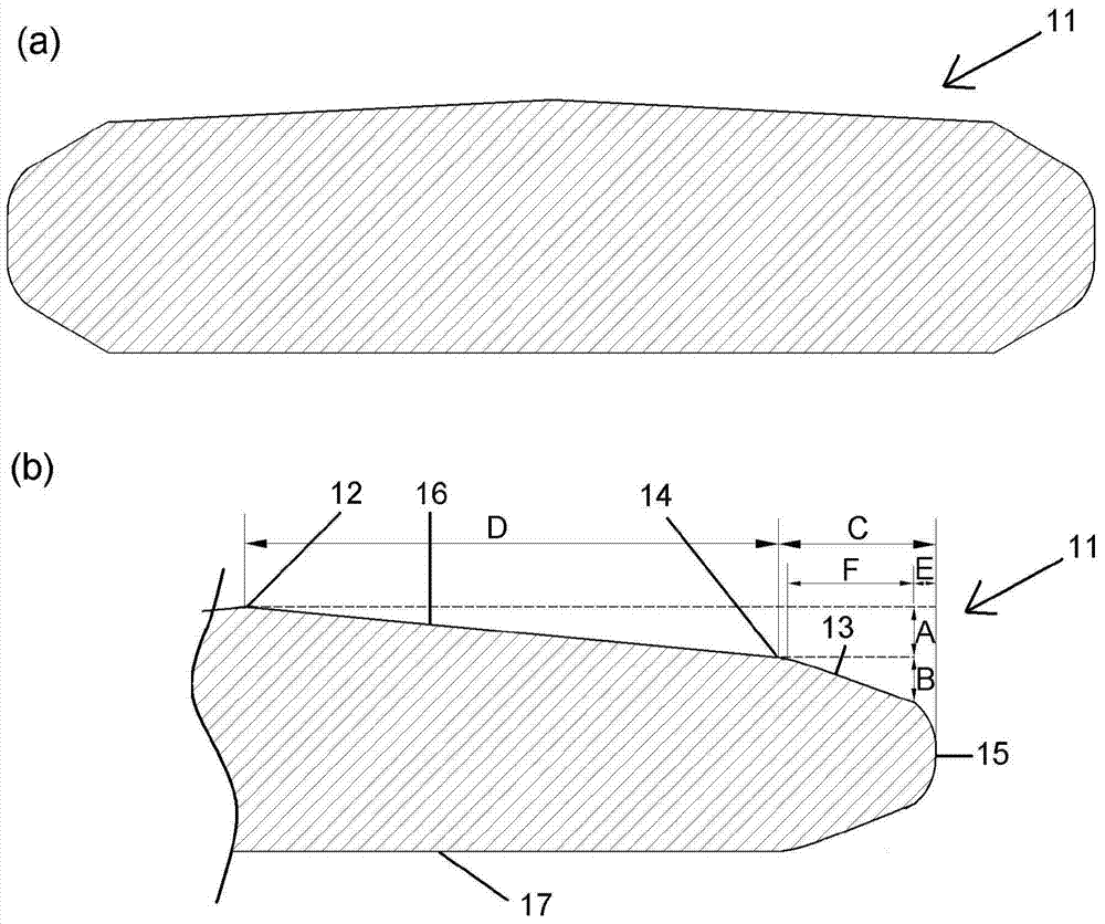
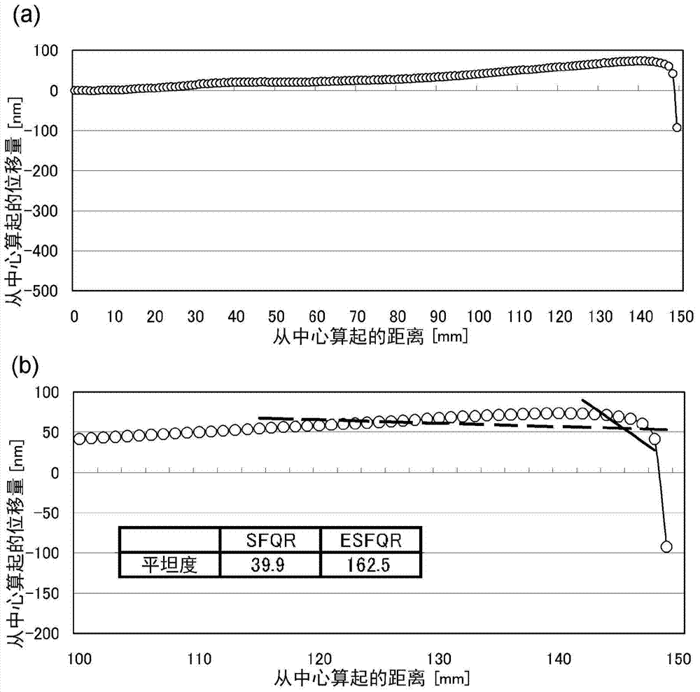
[0106] The single crystal rod was sliced ​​into silicon wafers with a diameter of 300 mm, and the silicon wafers were chamfered (chamfered) and planarized. Then, use the double-sided grinding machine described in Japanese Patent Application Laid-Open No. 2003-285262 and adjust to the following conditions to perform double-sided grinding: between the center of the semiconductor wafer and the peripheral sag start position, the thickness direction of the semiconductor wafer The amount of displacement is 100 nm or less, and the center of the semiconductor wafer has a convex shape. At this time, since it is not preferable to cause peripheral sagging due to double-sided polishing, a hard foamed urethane pad was used as a polishing cloth, specifically, MH-S15A manufactured by Nitta Haas was used. The abrasive slurry is made of colloidal silica with a particle size of 0.05 μm adjusted to pH 10.5, and the abrasive load is 200 g / cm 2for grinding. In order to stably obtain wafers with ...

Embodiment 2

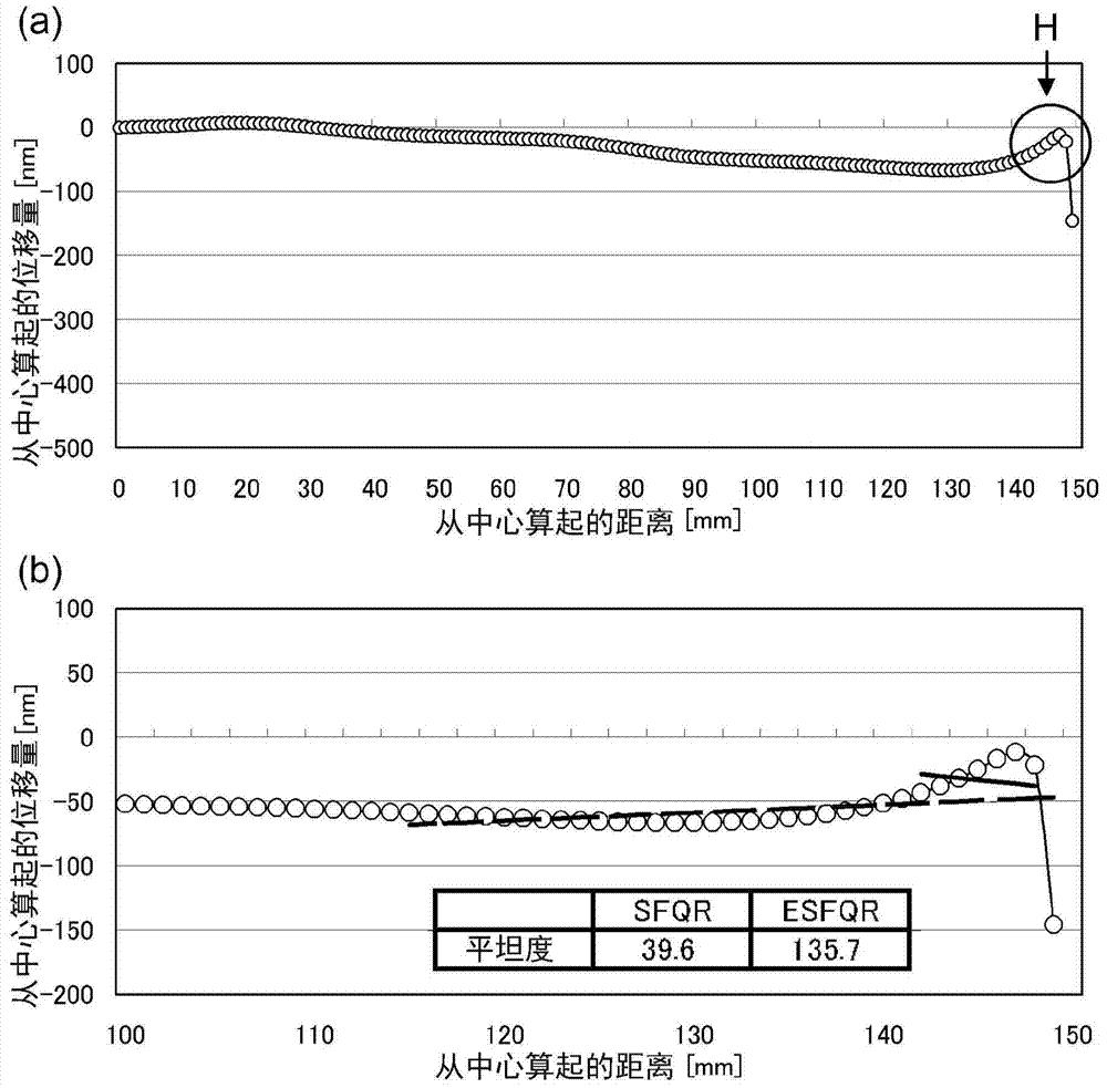
[0108] The surface temperature of the polishing cloth during polishing is relatively high in temperature at the central part of the polishing cloth compared with the outer peripheral part because heat is accumulated during polishing. This temperature difference will affect the grinding rate, so by controlling the range of this area, the starting position of sag can be controlled. In Example 2, in addition to adjusting the grinding load, the number of revolutions of the grinding head, and the slurry supply temperature in a manner that does not change the average in-plane grinding amount of the wafer, and increasing the area of ​​high temperature to be greater than that of Example 1, and to make The start position of the peripheral sag is closer to the center side (35mm from the outer peripheral end to the center side) than the outer peripheral portion of the semiconductor wafer that is the measurement object of ESFQR, except that one side of the silicon wafer is chemically mecha...


PUM


Abstract

A semiconductor wafer having sag formed at an outer periphery at the time of polishing, wherein a displacement of the semiconductor wafer in a thickness direction is 100 nm or less between a center and a outer peripheral sag start position of the semiconductor wafer, and the center of the semiconductor wafer has a convex shape, an amount of outer peripheral sag of the semiconductor wafer is 100 nm or less, and the outer peripheral sag start position is away from an outer peripheral portion of the semiconductor wafer toward the center or 20 mm or more away from an outer peripheral end of the semiconductor wafer toward the center, the outer peripheral portion being a measurement target of ESFQR.

Description

technical field [0001] The invention relates to a semiconductor wafer and a manufacturing method thereof. The semiconductor wafer satisfies two or more flatness parameters. Background technique [0002] In recent years, with the development of miniaturization, it is also required to have a flat wafer (wafer) shape up to the outer periphery of the semiconductor wafer. In addition to GBIR (Global Backsurface-referenced Ideal plane / Range, the overall back surface-reference Ideal plane / range), SFQR (Site Frontsurface referenced least sQuares / Range, site front referenced least squares / range), SBIR (Site Backsurface-referenced Ideal plane / Range, site back surface-reference ideal plane / range), etc., have also started The following new indicators are used: ROA (Roll Off Amount, also known as Edge Roll Off Amount) for evaluating the flatness of the peripheral portion of a semiconductor wafer, ESFQR (Edge Site Frontsurface referenced least sQuares / Range , frontal benchmark least squa...

Claims


Application Information

Patent Timeline
IPC IPC(8): H01L21/304
CPCH01L21/0201H01L21/02024H01L29/34B24B37/34H01L21/02H01L21/304
Inventor 佐藤三千登
Owner SHIN-ETSU HANDOTAI CO LTD
Features
  • Generate Ideas
  • Intellectual Property
  • Life Sciences
  • Materials
  • Tech Scout
  • Unparalleled Data Quality
  • Higher Quality Content
  • 60% Fewer Hallucinations
Learn More