Junction structure

一种接合结构体、接合层的技术,应用在焊接介质、焊接设备、电固体器件等方向,能够解决欠缺延展性、导热率等问题,达到防止裂缝的效果

Inactive Publication Date: 2014-01-01
PANASONIC CORP
View PDF7 Cites 5 Cited by
  • Summary
  • Abstract
  • Description
  • Claims
  • Application Information

AI Technical Summary

Problems solved by technology

[0005] Since the melting point of Bi-based solder material is around 270°C, there is no problem in terms of melting temperature, but it lacks ductility and thermal conductivity.
In addition, since the modulus of elasticity of Zn-based solder materials is too high, mechanical properties and heat resistance become problems in the internal bonding of semiconductor components.

Method used


Image

  • Junction structure
  • Junction structure
  • Junction structure

Examples


Embodiment approach 1

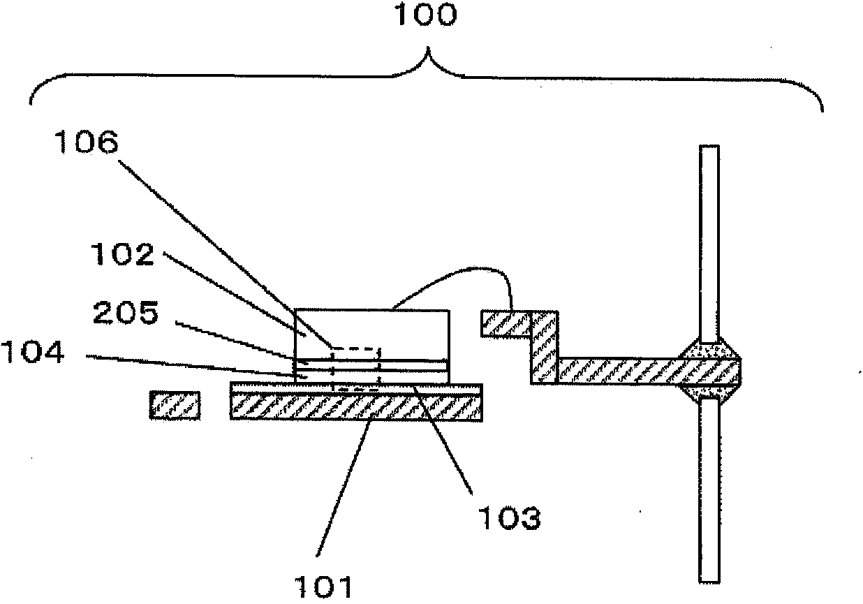
[0073] figure 1 It is a sectional view of the power semiconductor module 100 bonded by the bonding layer 104 according to the first embodiment. This power semiconductor module 100 includes: a substrate 101 ; and a semiconductor element 102 bonded to an electrode 103 on the substrate 101 via a bonding layer 104 . In addition, the junction structure 106 is constituted by the electrode 205 of the semiconductor element 102 , the junction layer 104 , and the electrode 103 .

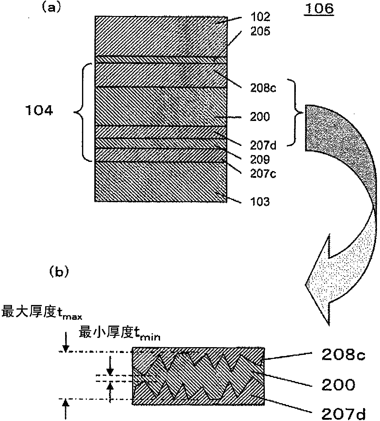
[0074] Next, use figure 2 (a) and (b) describe the formed joint structure 106 in detail. figure 2 (a) is a cross-sectional view showing a detailed cross-sectional structure of the bonded structure 106 . This junction structure 106 includes: an electrode 103 ; an electrode 205 of the semiconductor element 102 ; and a junction layer 104 that joins the electrode 103 and the electrode 205 . The bonding layer 104 is sequentially arranged from the electrode 103 side toward the electrode 205 side of the semico...

Embodiment approach 2

[0110] Figure 5 (a) is a cross-sectional view showing a detailed cross-sectional structure of the bonded structure 106 according to the second embodiment. Figure 5 (b) is Figure 5 (a) An enlarged cross-sectional view of the Cu layer 200. Figure 6 (a) to (c) are flowcharts of manufacturing steps of the bonded structure according to the second embodiment.

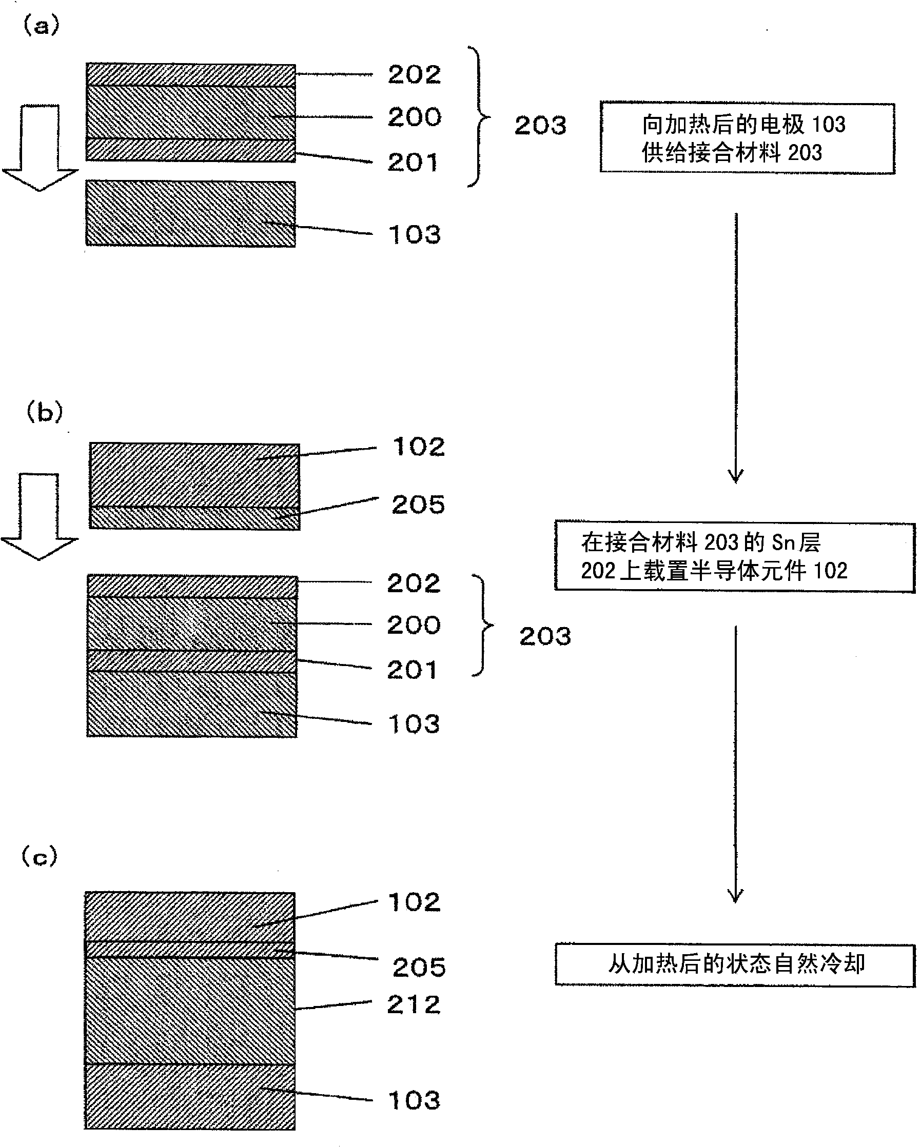
[0111] Such as Figure 5 As shown in (a), the junction structure 106 according to the second embodiment includes: the electrode 103 ; the electrode 205 of the semiconductor element 102 ; and the junction layer 104 between them. Such as Figure 6 As shown in the sectional view of (a), compared with the bonding material according to Embodiment 1, the bonding material 213 used in Embodiment 2 differs in that the electrode 103 side and the electrode 205 of the semiconductor element 102 are different. Meanwhile, the arrangement of the Sn—Bi layer 204 and the Sn layer 206 relative to the Cu layer 200 is an upside-down arra...

Embodiment approach 3

[0117] Figure 7 (a) is a cross-sectional view showing a detailed cross-sectional structure of the bonded structure 106 according to the third embodiment. This junction structure 106 includes: an electrode 103 ; an electrode 205 of the semiconductor element 102 ; and a junction layer 104 that joins the electrode 103 and the electrode 205 . The bonding layer 104 is sequentially arranged from the electrode 103 side toward the electrode 205 side of the semiconductor element 102: a first intermetallic compound layer 227 containing a CuSn-based intermetallic compound; a Bi layer 229; a second layer 227 containing a CuSn-based intermetallic compound. Cu layer 200; third intermetallic compound layer 228c containing a CuSn-based intermetallic compound; Bi layer 230; and fourth intermetallic compound layer 228d containing a CuSn-based intermetallic compound. and then, Figure 7 (b) is Figure 7 (a) Enlarged cross-sectional view of the three layers. as it should Figure 7 As shown ...


PUM

PropertyMeasurementUnit
melting pointaaaaaaaaaa

Abstract

A junction structure is provided with: an electrode of a substrate; an electrode of a semiconductor element; and a junction section that joins the electrode of the substrate, and the electrode of the semiconductor element. Starting from the electrode of the substrate and progressing toward the electrode of the semiconductor element, the following layers are placed in the following sequence in the junction section: a first intermetallic compound layer that contains a CuSn-based intermetallic compound; a Bi layer; a second intermetallic compound layer that contains a CuSn-based intermetallic compound; a Cu layer; and a third intermetallic compound layer that contains a CuSn-based intermetallic compound.

Description

technical field [0001] The invention relates to the internal bonding of semiconductor components. In particular, the present invention relates to a junction structure requiring excellent mechanical properties and heat resistance, including a junction layer that joins electrodes of a semiconductor element of a power semiconductor module and electrodes of a substrate. Background technique [0002] In the field of electronic device mounting, there is a desire for lead-free bonding due to concerns about the harmfulness of lead and environmental concerns, so materials that can replace Sn-Pb eutectic solder, which is a common solder material, are being developed and will be used The material is put into practice. [0003] On the other hand, against the background of technological progress of GaN and SiC, which are new-generation high-output devices that replace existing Si, as bonding materials for new-generation high-output devices, high heat-resistant Pb-free solder for devices...

Claims


Application Information

Patent Timeline
Patent Type & Authority Applications(China)
IPC IPC(8): H01L21/52B23K35/14H05K3/34
CPCH01L2224/83439H01L24/83B23K35/0272H01L2224/05639H01L24/29H01L2224/73265H01L2924/00014B23K35/22H01L2224/29147H01L23/49513H01L2224/83101H01L2224/48091H01L2924/01327H01L2224/29111H01L2224/83192H01L2224/8381H01L23/488H01L2924/3025H01L24/48H01L24/05H01L2224/32245H01L2224/05644H01L2224/83447H01L2224/04026H01L2924/01322H01L2224/05647H01L23/492H01L2224/48247H01L2224/29139H01L24/32H01L2224/05655H01L2224/29083H01L2924/00012H01L2924/00B23K35/264B23K35/302B23K35/0261H01L2224/04042H01L2224/27334H01L2224/83411H01L2224/05611H01L2224/2712H01L2224/32503H01L2224/32507H01L2224/83065H01L2224/83201H01L2224/83444H01L2224/83455H01L2224/83986H01L2924/351H01L2924/3512H01L2924/35121H01L2924/203H01L2924/12042H01L24/73H01L2224/45099H01L2924/01083H01L2224/8321H01L2924/0002
Inventor 中村太一北浦秀敏
Owner PANASONIC CORP
Why Eureka
Try Eureka