Blended crossing device for silicon-based nanowire

A crossbar, silicon-based nanotechnology, which is applied in the field of integrated photonics, can solve the problems that the manufacturing process increases the manufacturing cost of the device, limits the application range of the waveguide crossbar, and is not suitable for large-scale applications, so as to reduce crosstalk and diffraction loss. , Improve mode conversion efficiency, compact structure

Inactive Publication Date: 2014-01-15
SOUTHEAST UNIV
View PDF3 Cites 18 Cited by
  • Summary
  • Abstract
  • Description
  • Claims
  • Application Information

AI Technical Summary

Problems solved by technology

For example, the mode-extended crossover scheme is used to limit the mode field at the waveguide intersection to a larger range to reduce loss and crosstalk, but the double-etching manufacturing process increases the manufacturing cost of the device
In addition, using a vertical manufacturing process to manufacture waveguide interleavers can obtain better device performance, but compared with planar technology, this manufacturing method is obviously much more complicated and the manufacturing cost is relatively high
Although these solutions can reduce the loss and crosstalk of the waveguide crossover to varying degrees and improve the performance of the device, they are difficult to manufacture and are not suitable for large-scale applications, and the crossover design methods are only for a single type of strip structure waveguide. , which greatly limits the application range of waveguide interleavers

Method used


Image

  • Blended crossing device for silicon-based nanowire
  • Blended crossing device for silicon-based nanowire
  • Blended crossing device for silicon-based nanowire

Examples


Embodiment Construction

[0024] The principles and features of the present invention will be described below in conjunction with the accompanying drawings, and the examples given are only used to explain the present invention and are not intended to limit the scope of the present invention.

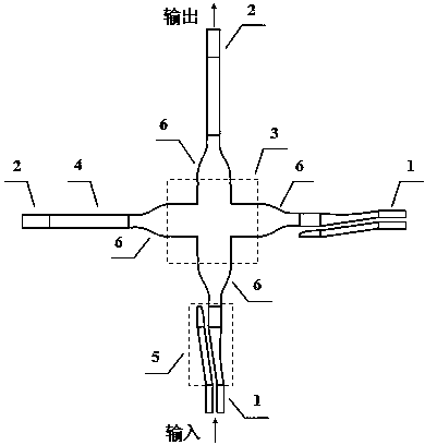
[0025] Such as figure 1 As shown, a silicon-based nanowire hybrid crossover device of the present invention includes two slot waveguide mode conversion units, two strip waveguide mode conversion units, a sinusoidal conversion waveguide 6 and a cross multimode waveguide 3 . The two slot waveguide mode conversion units and the two strip waveguide mode conversion units are respectively connected to the cross multimode waveguide 3 through the sinusoidal conversion waveguide 6 . Each groove waveguide mode conversion unit is opposed to one strip waveguide mode conversion unit. Each slot waveguide mode conversion unit includes a slot waveguide 1 for optical signal input and a mode converter 5 connected between the slot...


PUM


Abstract

The invention discloses a blended crossing device for a silicon-based nanowire. The crossing device comprises two groove waveguide mode switching units, two slab waveguide mode switching units, a sine switching waveguide and a crossing multimode waveguide, wherein the two groove waveguide mode switching units and the two slab waveguide mode switching units are respectively connected through the sine switching waveguide and the crossing multimode waveguide, each groove waveguide mode switching unit is opposite to one slab waveguide mode switching unit, each groove waveguide mode switching unit comprises a groove waveguide for inputting an optical signal and a mode switcher, each mode switcher is connected between each groove waveguide and the sine switching waveguide, each slab waveguide mode switching unit comprises a slab waveguide and a single-mode waveguide for outputting the optical signal, and each single-mode waveguide is connected between each slab waveguide and the sine switching waveguide. The crossing device has the advantages of high transmission efficiency, compact structure, low loss, low manufacturing difficulty, relatively low cost and the like.

Description

technical field [0001] The invention belongs to the technical field of integrated photonics, and in particular relates to a silicon-based nanowire hybrid crosser. Background technique [0002] As a kind of functional device in photonic integrated circuits, waveguide interleavers play an important role in signal routing and improving the integration of devices. Direct planar waveguide crossing, due to the obvious diffraction effect of the optical field at the center of the waveguide crossing, the loss and crosstalk are greatly increased. Especially for materials with high refractive index difference such as silicon-on-insulator, the loss and crosstalk are very serious, which greatly affects the performance of waveguide interleavers and restricts its application in the field of integrated optical devices. Therefore, it is very important to develop a waveguide crossover that meets the application requirements. In recent years, researchers have conducted a lot of research on w...

Claims


Application Information

Patent Timeline
Patent Type & Authority Applications(China)
IPC IPC(8): G02B6/125
Inventor 肖金标徐银
Owner SOUTHEAST UNIV
Why Eureka
Try Eureka