Manufacturing method of OLED of double-face submicron order structure

A sub-micron-scale, manufacturing method technology, applied in the direction of organic light-emitting device manufacturing/processing, semiconductor/solid-state device manufacturing, organic light-emitting devices, etc., can solve difficult large-area preparation, high cost of quartz substrate patterning, and low light extraction efficiency and other problems to achieve the effect of improving the transmittance

Inactive Publication Date: 2014-01-15
XI AN JIAOTONG UNIV
View PDF4 Cites 3 Cited by
  • Summary
  • Abstract
  • Description
  • Claims
  • Application Information

AI Technical Summary

Problems solved by technology

[0004] In order to overcome the defects of the above-mentioned prior art, the object of the present invention is to provide a method for manufacturing OLEDs with a double-sided submicron structure on a qu

Method used


Image

  • Manufacturing method of OLED of double-face submicron order structure
  • Manufacturing method of OLED of double-face submicron order structure
  • Manufacturing method of OLED of double-face submicron order structure

Examples


Embodiment Construction

[0029] The present invention will be further described in detail below in conjunction with specific drawings and embodiments, which are explanations rather than limitations of the present invention.

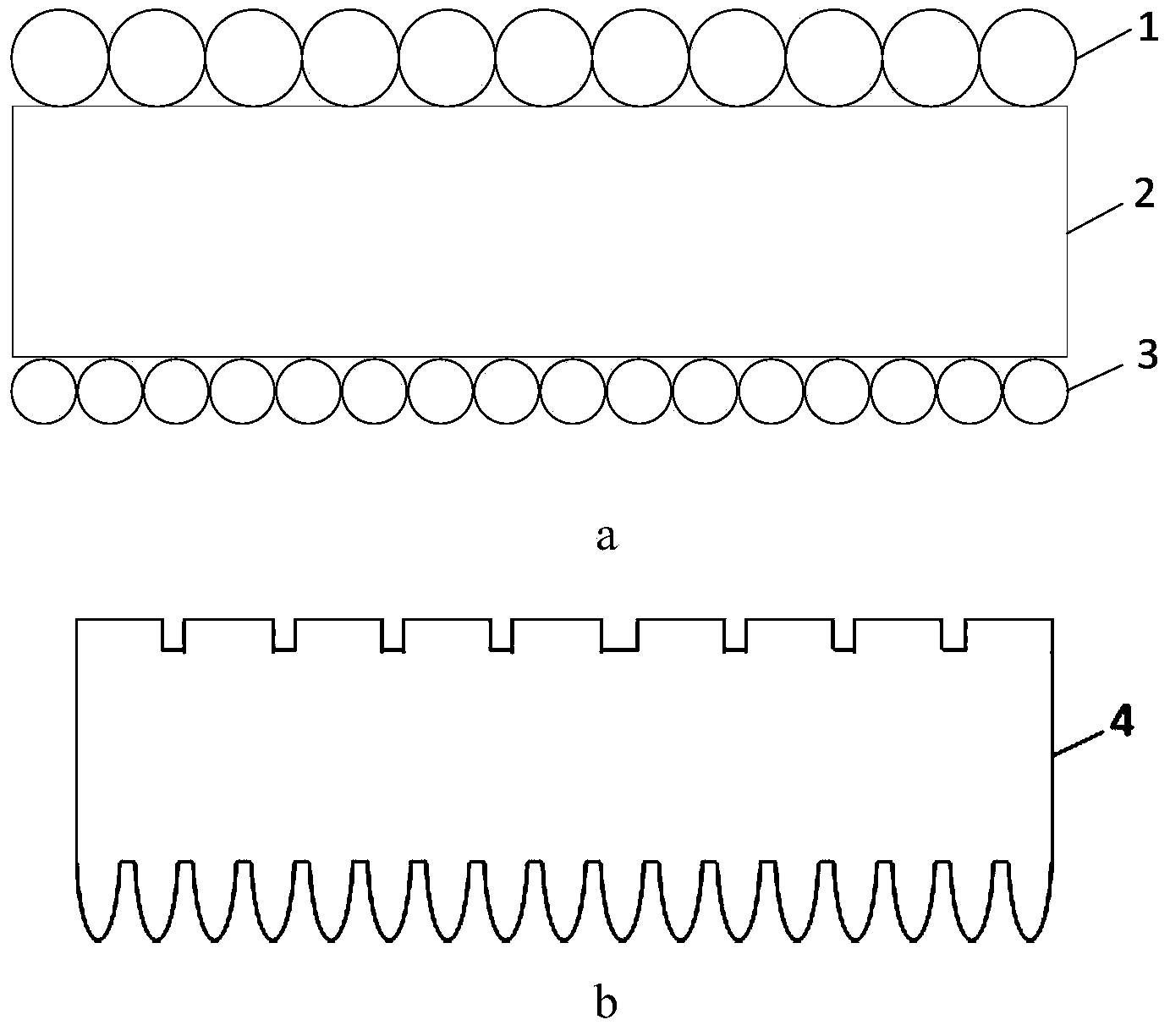
[0030] Quartz substrate of the present invention has the manufacture method of the OLED device of double-sided submicron structure, comprises the following steps:

[0031] 1) Cleaning of quartz substrate

[0032] Clean the quartz substrate 2 with a detergent, put the quartz substrate 2 into acetone solution, ethanol solution, and deionized water in sequence, ultrasonically clean each for 5 to 15 minutes, and then place the quartz substrate on a hot plate to dry;

[0033] 2) if figure 1 As shown in a, the silicon dioxide ball 1 with a particle size of 400nm and the silicon dioxide ball 3 with a particle size of 200nm were spin-coated on both sides of a quartz substrate 2 by spin coating, and made into a single surface. Layer arrangement, due to the uneven particle size of the si...


PUM

PropertyMeasurementUnit
Particle sizeaaaaaaaaaa

Abstract

The invention discloses a manufacturing method of an OLED of a double-face submicron order structure, and belongs to the technical field of OLED manufacturing. The method includes the following steps: (1) the two faces of a quartz substrate are simultaneously coated by single-layer silicon dioxide nanoballs in a spinning mode; (2) the well-distributed single-layer silicon dioxide nanoballs serve as masks, submicron order graph structures are etched on the two faces of the quartz substrate; (3) the quartz substrate with the submicron order graph structures is evenly coated by an ITO conductive film in a spinning mode to obtain an OLED anode; (4) an electron hole conveying layer, an evaporation light-emitting layer and an electronic conveying layer are sequentially evaporated on the OLED anode, finally a cathode is evaporated and the OLED of the double-face submicron order structure is obtained. The quartz substrate manufactured in the method has an OLED component of a double-face structure, a light-emitting model of the quartz substrate is close to a Lambert reflector, spectral line deviation and obvious angle dependence do not exist, the optical extraction efficiency of the component is improved, and meanwhile, performance regression does not occur.

Description

technical field [0001] The invention belongs to the technical field of OLED manufacture, and in particular relates to a method for manufacturing an OLED with a double-sided submicron structure. Background technique [0002] Since the first paper on organic electroluminescent devices was published by Tang et al. in 1987, this new type of electronic devices has attracted extensive attention from academia and industry. After more than 20 years of hard work, organic electroluminescent devices have gradually entered daily life as commercial products. The efficiency of the device itself is also an important indicator of OLED performance. OLED device efficiency can be divided into internal quantum efficiency and external quantum efficiency. The efficiency of converting electrical energy into visible light through a device is called the internal quantum efficiency. Through the study of phosphorescent triplet light-emitting materials, the internal quantum efficiency of the device ca...

Claims


Application Information

Patent Timeline
IPC IPC(8): H01L51/56
CPCH10K71/00
Inventor 王莉丁玉成罗钰李龙严诚平卢秉桓
Owner XI AN JIAOTONG UNIV
Why Eureka
Try Eureka