Method for removing GaN-based epitaxial layer on substrate

A technology of epitaxial layer and substrate, which is applied in the direction of electrical components, circuits, semiconductor devices, etc., can solve the problems of unsuitable patterned substrates, high polishing precision requirements, substrate lattice damage, etc., and achieve good uniformity of photoelectric parameters , crystal quality is good, the effect is good

Inactive Publication Date: 2014-01-22
HANGZHOU SILAN AZURE
View PDF4 Cites 5 Cited by
  • Summary
  • Abstract
  • Description
  • Claims
  • Application Information

AI Technical Summary

Problems solved by technology

However, this type of method has high grinding costs, reduced substrate thickness after grinding (may not be conducive to repeated use), high polishing precision requirements, easy to cause substrate lattice damage, and is not suitable for patterned substrates

Method used


Image

  • Method for removing GaN-based epitaxial layer on substrate
  • Method for removing GaN-based epitaxial layer on substrate
  • Method for removing GaN-based epitaxial layer on substrate

Examples


Embodiment Construction

[0025] The present invention will be further described below in conjunction with specific embodiments and accompanying drawings, but the protection scope of the present invention should not be limited thereby.

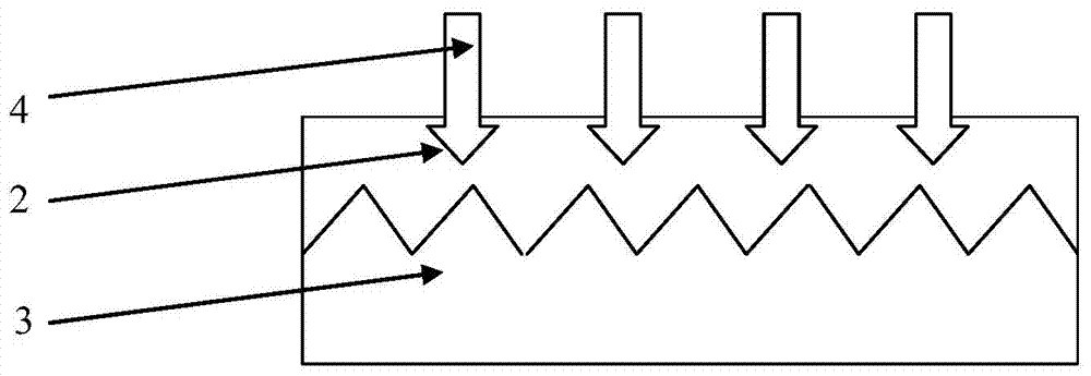
[0026] The invention provides a method for removing a GaN-based epitaxial layer on a substrate, wherein the substrate and the GaN-based epitaxial layer on the substrate form an epitaxial wafer. The present invention uses chlorine (CL 2 ) to etch away the GaN-based epitaxial layer on the substrate, thereby obtaining a substrate from which the GaN-based epitaxial layer has been removed.

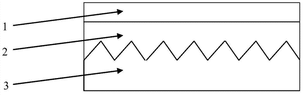
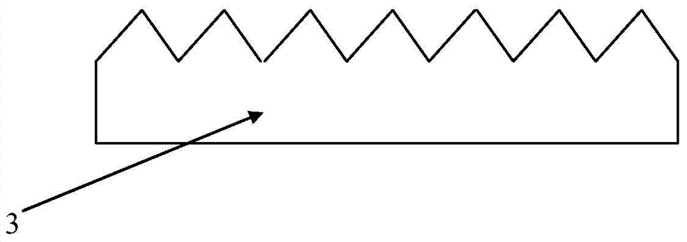
[0027] figure 1 A schematic cross-sectional view of an epitaxial wafer that may be used in one embodiment of the invention is shown. As those skilled in the art can understand, an epitaxial wafer refers to a structure in which an epitaxial layer 2 is grown on a substrate 3 , including a structure in which epitaxial materials are attached to other substrates or pedestals. In some embo...


PUM


Abstract

The invention provides a method for removing a GaN-based epitaxial layer on a substrate. The substrate and the GaN-based epitaxial layer on the substrate form an epitaxial wafer. The method comprises the steps as follows: putting the epitaxial wafer in a reaction cavity and introducing chlorine gas (CL2) into the reaction cavity, wherein the chlorine gas (CL2) is used for reacting with the GaN-based epitaxial layer at a preset temperature and a preset cavity pressure in the reaction cavity to etch the GaN-based epitaxial layer, but the substrate does not react with the chlorine gas (CL2), so that the substrate with the GaN-based epitaxial layer removed is obtained. According to the invention, the substrate with the GaN-based epitaxial layer removed can be used for epitaxial growth again.

Description

technical field [0001] The invention relates to the field of semiconductor chip manufacturing, in particular to a method for removing a GaN-based epitaxial layer on a substrate. Background technique [0002] Light-emitting diodes based on nitride-based semiconductor materials have the advantages of high brightness, long life, energy saving, etc., and therefore have a wide range of applications in the fields of display and lighting. One technique for realizing GaN substrates is by vapor deposition methods such as hydride vapor phase epitaxy, or HVPE, on sapphire (Al 2 o 3 ) or a silicon carbide (SiC) substrate to grow a thicker gallium nitride (GaN) epitaxial layer, and then manufacture LEDs on the GaN epitaxial layer. [0003] Sapphire crystal (Al 2 o 3 ) is a high-quality material with high temperature resistance, wear resistance and corrosion resistance. It is mainly used as a semiconductor substrate and a large-scale integrated circuit substrate. It can be used in mic...

Claims


Application Information

Patent Timeline
Patent Type & Authority Applications(China)
IPC IPC(8): H01L33/00H01L21/465
CPCH01L33/0093
Inventor 蒋伟李东昇徐小明江忠永
Owner HANGZHOU SILAN AZURE
Why Eureka
Try Eureka