Formation method of metal gate

A metal gate, metal layer technology, applied in electrical components, semiconductor/solid-state device manufacturing, semiconductor devices, etc., can solve the problems of easy leakage current, affect transistor stability, high temperature, reduce the occupied space, The effect of improving speed and efficiency

Inactive Publication Date: 2014-01-29
SEMICON MFG INT (SHANGHAI) CORP
View PDF4 Cites 2 Cited by
  • Summary
  • Abstract
  • Description
  • Claims
  • Application Information

AI Technical Summary

Problems solved by technology

[0008] However, as the size of the device continues to decrease, the impedance of the metal gate formed by the above method will become larger, and leakage current will easily occur, which will affect the stability of the transistor. In order to solve the above problems, the US patent application number US6080646A proposes a A method for forming a metal gate, comprising: providing a semiconductor substrate on which a dummy gate is formed; forming a dielectric layer on the semiconductor substrate, the surface of the dielectric layer being flush with the surface of the dummy gate; An aluminum metal layer is formed on the surface of the gate and the dielectric layer; annealing is performed, and the polysilicon in the dummy gate is exchanged with the aluminum in the aluminum metal layer to form a metal gate; the alternating polysilicon and part of the unreacted aluminum layer are removed
[0009] However, in the above-mentioned method of forming an aluminum metal gate, the interaction rate and efficiency of aluminum and polysilicon are low, and the annealing temperature is relatively high

Method used


Image

  • Formation method of metal gate
  • Formation method of metal gate
  • Formation method of metal gate

Examples


no. 1 example

[0045] refer to Figure 4 , Figure 4 It is a schematic flowchart of a method for forming a metal gate according to the first embodiment of the present invention, including the steps:

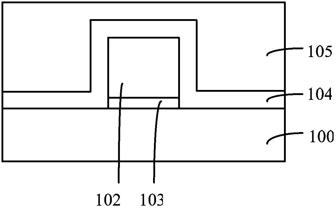
[0046] Step S21, a semiconductor substrate is provided, a dummy gate is formed on the semiconductor substrate, a gate dielectric layer is formed between the semiconductor substrate and the dummy gate, and the gate dielectric layer is a stack of an interface layer and a high-K dielectric layer structure;

[0047] Step S22, forming a dielectric layer on the surface of the semiconductor substrate, and the surface of the dielectric layer is flush with the surface of the dummy gate;

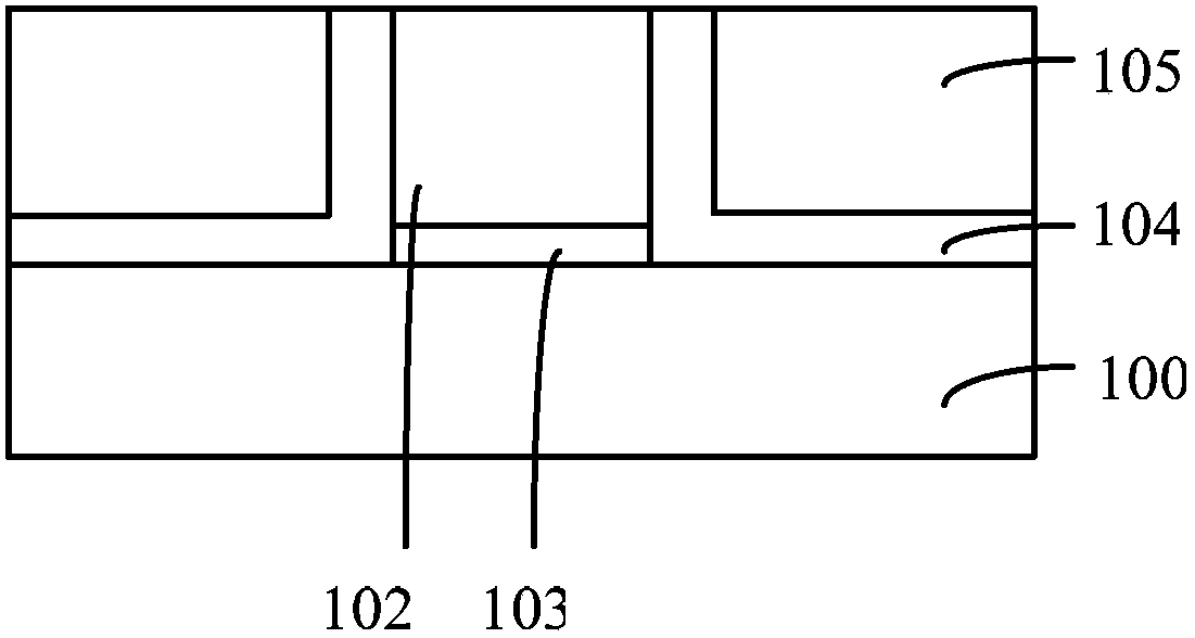
[0048] Step S23, removing the dummy gate, forming a groove, and forming a functional layer on the bottom and sidewalls of the groove;

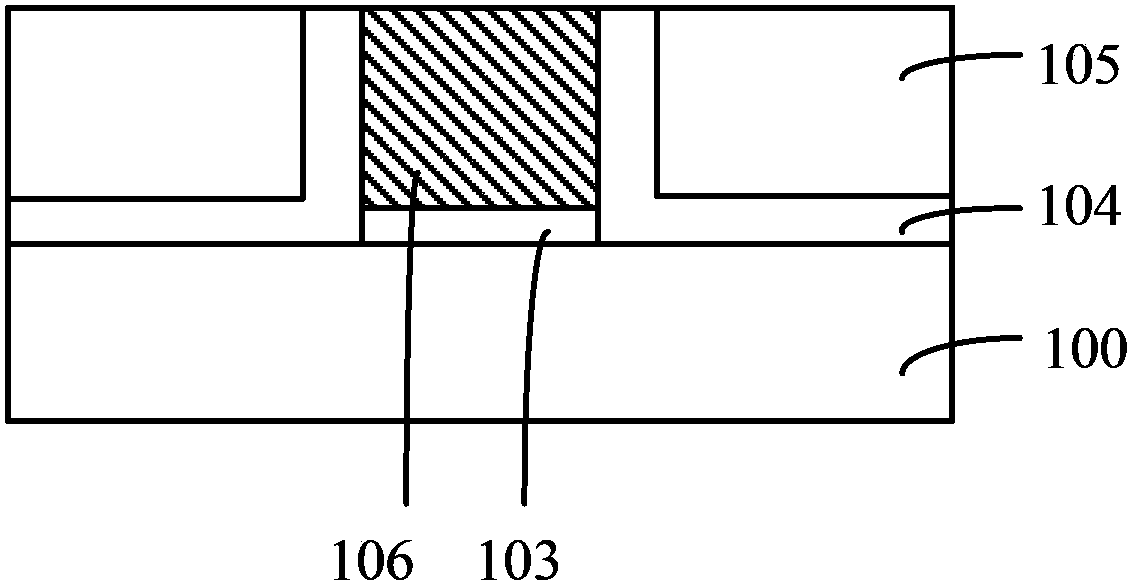
[0049] Step S24, a silicon material layer is formed on the surface of the functional layer in the groove, and the surface of the silicon material layer is flush with the surface of ...

no. 2 example

[0085] refer to Figure 13 , Figure 13 It is a schematic flowchart of a method for forming a metal gate according to the second embodiment of the present invention, including the steps:

[0086] Step S31, providing a semiconductor substrate, the semiconductor substrate includes a first region and a second region, a first dummy gate is formed on the first region of the semiconductor substrate, and a first dummy gate is formed on the second region of the semiconductor substrate There is a second pseudo gate;

[0087] Step S32, forming a dielectric layer on the surface of the semiconductor substrate, and the surface of the dielectric layer is flush with the surfaces of the first dummy gate and the second dummy gate;

[0088] Step S33, removing the first dummy gate, forming a first groove, and forming a first functional layer on the bottom and sidewalls of the first groove;

[0089] Step S34, forming a first silicon material layer on the surface of the first functional layer, ...


PUM

PropertyMeasurementUnit
thicknessaaaaaaaaaa
thicknessaaaaaaaaaa

Abstract

A formation method of a metal gate includes: providing a semiconductor substrate and forming pseudo gates on the semiconductor substrate; forming a dielectric layer on the surface of the semiconductor substrate; flushing the surface of the dielectric layer and the surfaces of the pseudo gate; removing the pseudo gates to form grooves, and forming functional layers at the bottoms and the side walls of the grooves; forming silicon layers on the surfaces of the functional layers in the grooves, wherein the surfaces of the silicon layers are flush with the surfaces of the dielectric layer; forming an aluminum metal layer on the surface of the dielectric layer and the surfaces of the silicon layers; forming a silicon-capture metal layer on the surface of the aluminum metal layer; annealing the semiconductor substrate, wherein aluminum in the aluminum metal layer and silicon in the silicon layers are exchanged to form the metal gate, and the exchanged silicon and metal in the silicon-capture metal layer are reacted to form a metal silicon compound. The exchanged silicon is consumed by the silicon-capture metal layer, so that speed and efficiency of silicon exchange in the aluminum and silicon layers in the aluminum metal layer are accordingly increased.

Description

technical field [0001] The invention relates to the field of semiconductor fabrication, in particular to a method for forming an aluminum metal gate. Background technique [0002] With the continuous development of integrated circuit manufacturing technology, the feature size of MOS transistors is getting smaller and smaller. In order to reduce the parasitic capacitance of the MOS transistor gate and improve the device speed, the gate stack of the high-K gate dielectric layer and the metal gate is required. Structures are introduced into MOS transistors. In order to avoid the influence of the metal material of the metal gate on other structures of the transistor, the gate stack structure of the metal gate and the high-K gate dielectric layer is usually fabricated by a “gate last” process. [0003] Figure 1~Figure 3 It is a schematic diagram of a cross-sectional structure of a metal gate fabricated by an existing "gate last" process. [0004] refer to figure 1 , providin...

Claims


Application Information

Patent Timeline
Patent Type & Authority Applications(China)
IPC IPC(8): H01L21/28
CPCH01L21/28097H01L21/28176
Inventor 洪中山平延磊
Owner SEMICON MFG INT (SHANGHAI) CORP
Why Eureka
Try Eureka