Light emitting device, lighting device, and display device

A technology for light-emitting devices and light-emitting parts, which is applied to lighting devices, lighting device parts, lighting and heating equipment, etc., can solve the problems of light attenuation, large restrictions, and inability to display images in small divided areas, and achieve thinning. Effect

Inactive Publication Date: 2014-01-29
SHARP KK
View PDF8 Cites 13 Cited by
  • Summary
  • Abstract
  • Description
  • Claims
  • Application Information

AI Technical Summary

Problems solved by technology

However, the edge-lit backlight unit not only has the problem of concentrated heat generation of the light sources due to the concentrated arrangement of the light sources at the edge of the light guide plate, but also has the problem of increasing the size of the frame of the display panel.
Furthermore, the edge-light type backlight unit has the problem that local dimming control (local dimming) that has attracted attention as a control method that can realize high-quality display images and power saving Control of small segmented areas to achieve high quality display images and power saving
However, in the technologies disclosed in Patent Documents 1 to 5, the amount of light changes with the square of the distance from the light-emitting element, so the light amount attenuates at the corner far from the light-emitting element compared with other positions, and it cannot provide surface orientation. On the uniform amount of light, so can not fully meet the above requirements

Method used


Image

  • Light emitting device, lighting device, and display device
  • Light emitting device, lighting device, and display device
  • Light emitting device, lighting device, and display device

Examples


Embodiment Construction

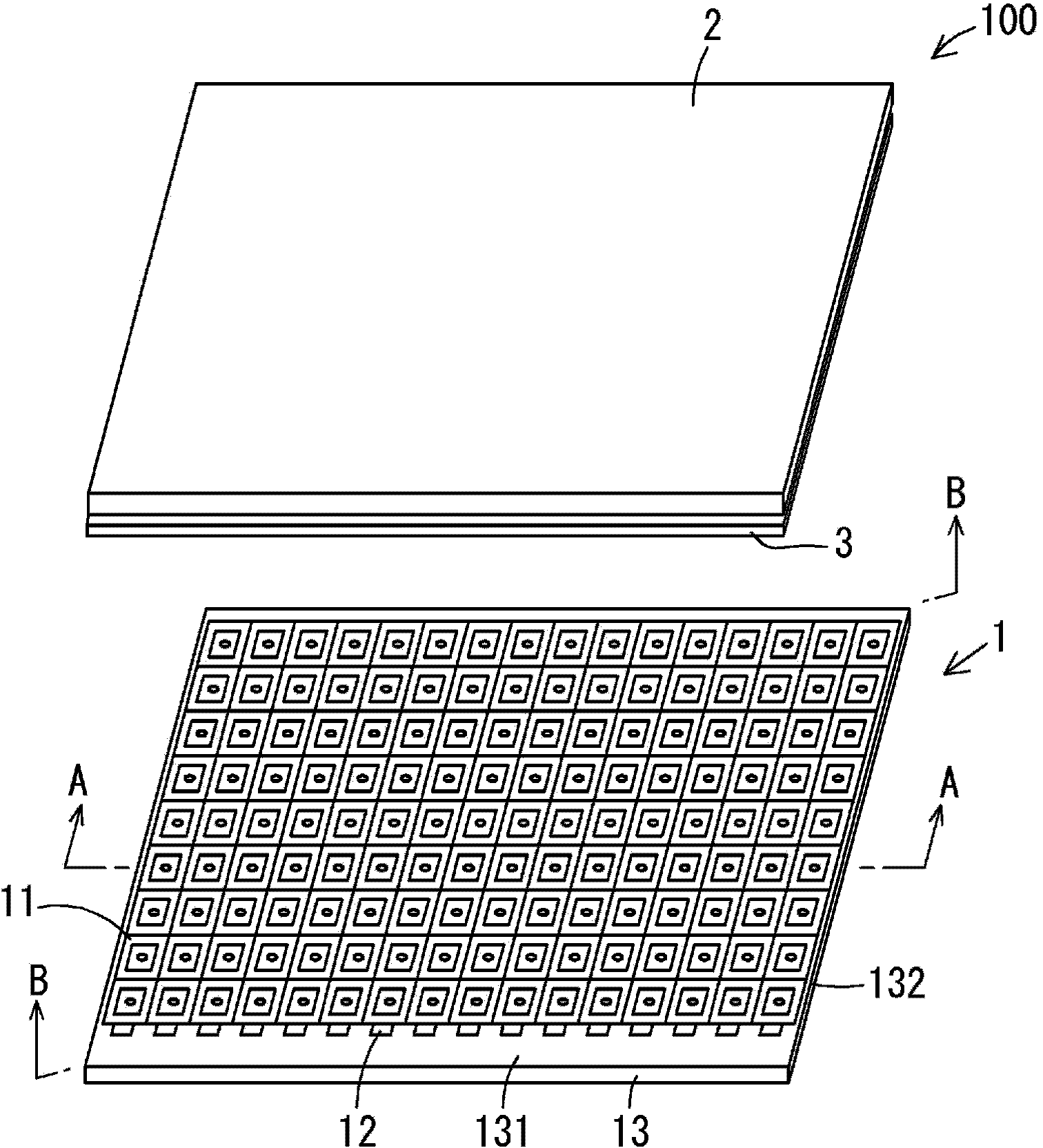
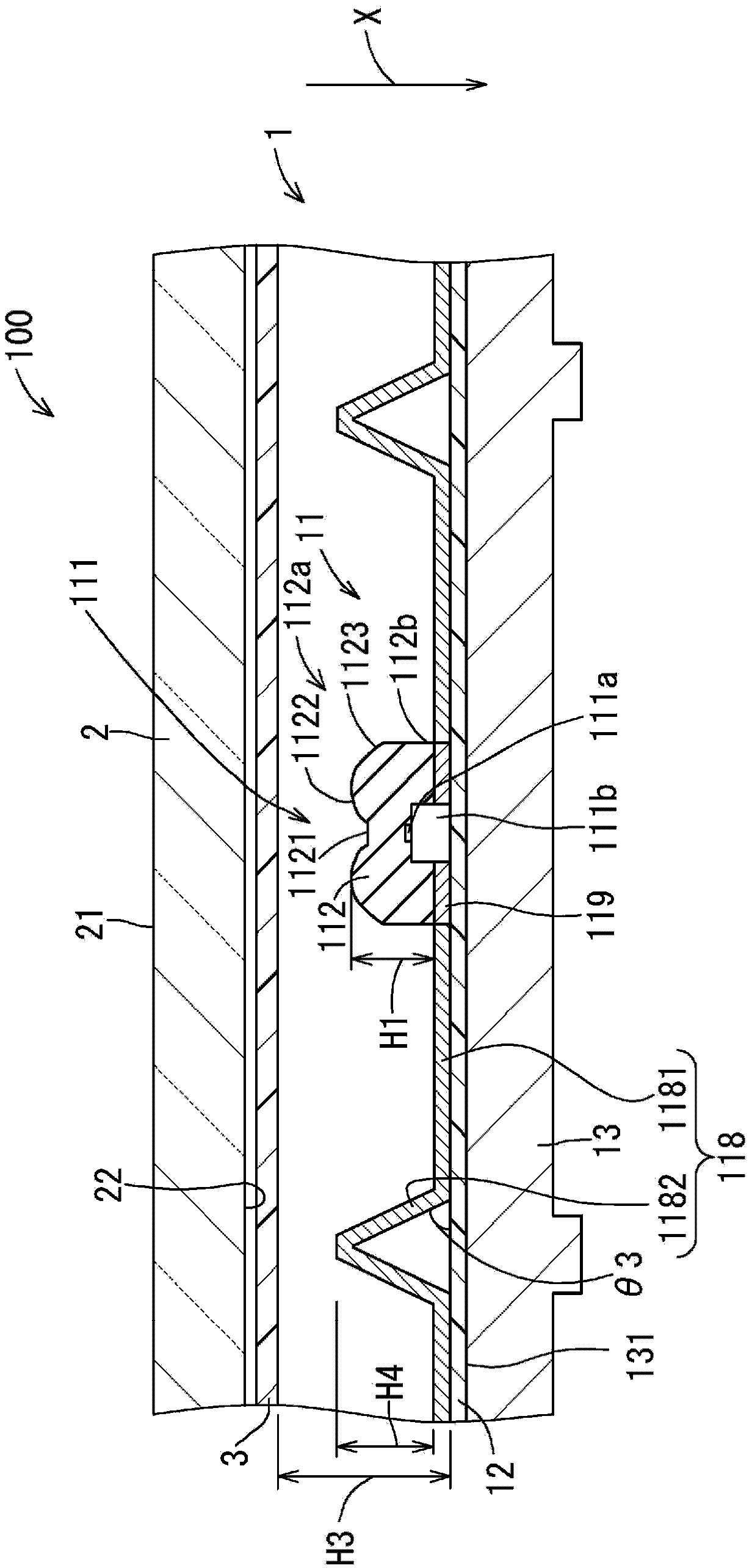
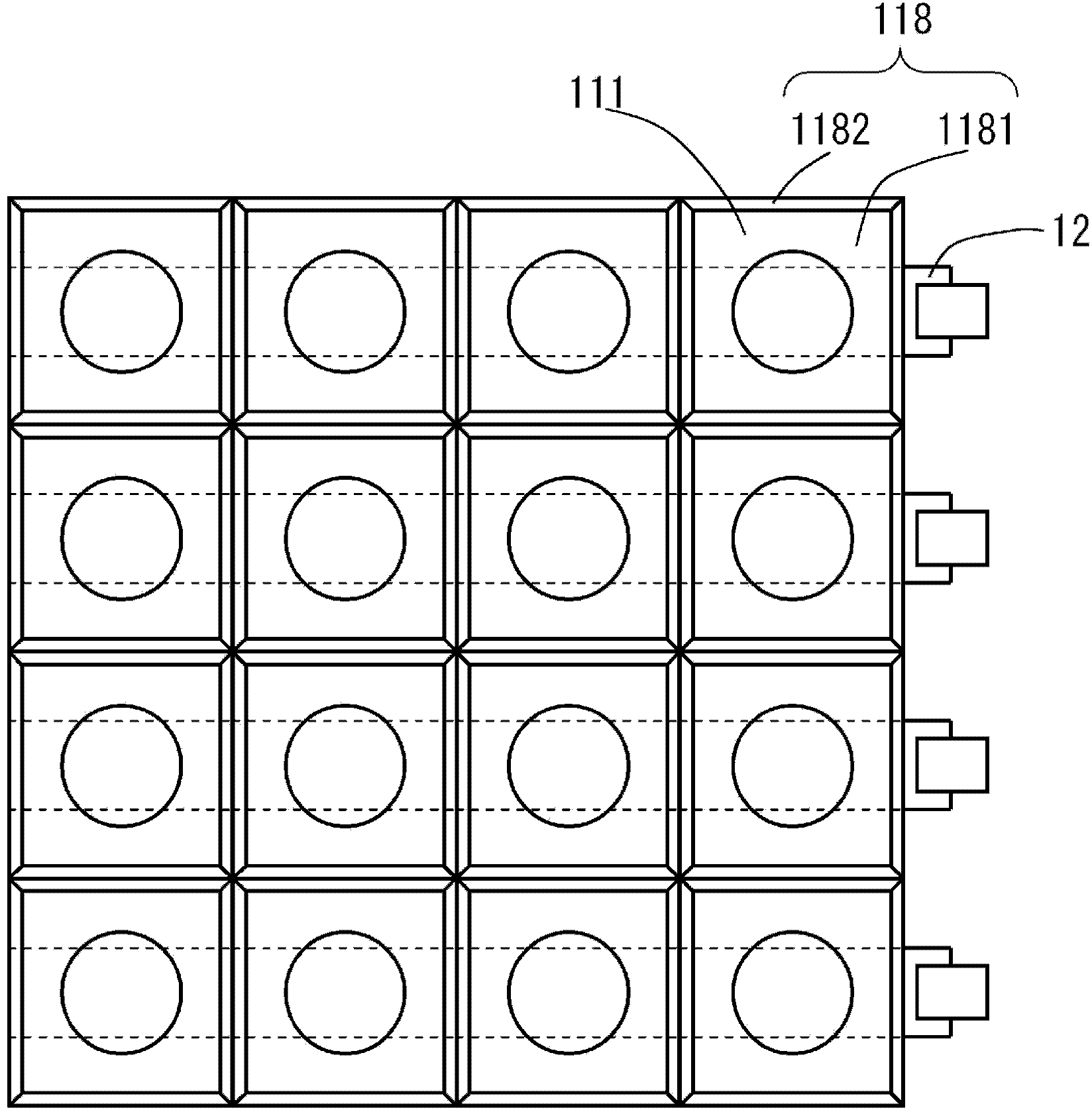
[0080] figure 1 It is an exploded perspective view showing the configuration of the liquid crystal display device 100 according to the basic structure of the present invention. Figure 2A is indicative of the figure 1 A cross-sectional view of the liquid crystal display device 100 when the cutting plane line A-A in FIG. The liquid crystal display device 100 which is a display device of the present invention is a device that displays an image on a display screen by outputting image information to a television, a personal computer, or the like. The display screen is formed by a liquid crystal panel 2 that is a transmissive display panel having a liquid crystal element, and the liquid crystal panel 2 is formed in a rectangular flat plate shape. In the liquid crystal panel 2 , two orientations in the thickness direction are defined as the front 21 side and the back 22 side. The liquid crystal display device 100 displays images recognizably when viewed from the front 21 side.

...


PUM

PropertyMeasurementUnit
heightaaaaaaaaaa
thicknessaaaaaaaaaa
thicknessaaaaaaaaaa

Abstract

The present invention is a light emitting device used in a back light unit for a display device provided with a display panel. The present invention is specifically a light emitting device wherein light can be shown onto an object that is illuminated in the direction of the surface of that object that is illuminated with uniform brightness and that can be made thin and is also a lighting device and a display device provided with this light emitting device. A back light unit (1) is provided with a printed circuit board (12), a plurality of light emitting units (111) provided on the printed circuit board (12) and having a base (111b), an LED chip (111a), and a lens (112), and a reflective member (113) provided around the light emitting units (111) and having a first reflective member (1131) and a second reflective member (1132).

Description

technical field [0001] The present invention relates to a light emitting device provided in a backlight unit for irradiating light on the back surface of a display panel, and an illuminating device and a display device including the light emitting device. Background technique [0002] In the display panel, liquid crystal is sealed between two transparent substrates, and the direction of the liquid crystal molecules is changed by applying a voltage to change the light transmittance, thereby optically displaying a predetermined image or the like. In this display panel, since the liquid crystal itself is not a luminous body, for example, on the back side of a transmissive display panel, there is a device for irradiating light from a cold cathode tube (CCFL), a light emitting diode (LED: Light Emitting Diode), etc. as a light source. backlight components. [0003] Among the backlight units, there are: a direct type in which light sources such as cold cathode tubes or LEDs are a...

Claims


Application Information

Patent Timeline
Patent Type & Authority Applications(China)
IPC IPC(8): H01L33/60F21S2/00G02F1/13357H01L33/54H01L33/58F21Y101/02
CPCG02F1/133605H01L33/60H01L33/54G02F2001/133612G02F2001/133607H01L2224/48091G02F1/133603G02F1/133611H01L33/58G02F1/133612G02F1/133607H01L2924/1815H01L2924/00014F21K9/20H01L33/483F21Y2115/10F21V7/04
Inventor 和田孝澄小野泰宏增田麻言大久保宪造白井伸弘
Owner SHARP KK
Why Eureka
Try Eureka