A push-up mechanism and a lithography device with the push-up mechanism

A technology of push pins and driving devices, which is applied in the direction of photolithography exposure devices, microlithography exposure equipment, etc., can solve the problems of low product yield, long handover time, broken silicon wafers/glass substrates, etc., to improve production efficiency and reduce handover time

Active Publication Date: 2016-03-09
SHANGHAI MICRO ELECTRONICS EQUIP (GRP) CO LTD
View PDF12 Cites 2 Cited by
  • Summary
  • Abstract
  • Description
  • Claims
  • Application Information

AI Technical Summary

Problems solved by technology

[0007] The present invention aims at various deficiencies in the prior art, improves the structure of the ejector mechanism, and improves the deficiencies in the prior art of long handover time, low product yield, and the risk of breakage of silicon wafers / glass substrates

Method used


Image

  • A push-up mechanism and a lithography device with the push-up mechanism
  • A push-up mechanism and a lithography device with the push-up mechanism
  • A push-up mechanism and a lithography device with the push-up mechanism

Examples


Embodiment 1

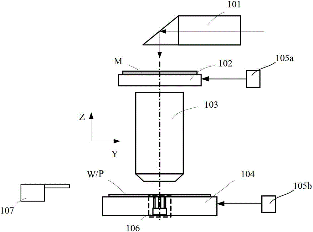
[0022] see image 3 , this embodiment firstly describes the structure of the photolithography machine schematically. As can be seen from the figure, the lithography machine mainly includes an illumination system 101, a mask table 102, a projection objective lens 103, a workpiece table 104, laser interferometers 105a, 105b, an ejector mechanism 106, and a wafer / substrate transfer system 107. The illumination system 101 provides the exposure light source for the exposure device, the mask stage 102 supports and positions the reticle M, and the projection objective lens 103 provides the exposure field of view, exposing the pattern on the reticle M on the silicon wafer / glass substrate W / P (Wafer / Plate ), the workpiece table 104 carries the silicon wafer / glass substrate W / P, and provides support and positioning functions for the silicon wafer / glass substrate W / P. Laser interferometers 105 a , 105 b provide position signals for precise motion control of mask table 102 and workpiece ...

Embodiment 2

[0027] Figure 5 It is a structural schematic diagram of Embodiment 2 of the ejecting mechanism of the present invention. By several sets of reed mechanisms 301a, 301b ( Figure 5 Only two groups are drawn) to form an elastic damping device, so that the entire ejector mechanism joint / plate part has a certain stiffness K and damping C in the vertical direction, which provides protection for the silicon wafer / glass substrate when the piece / plate is unloaded, and at the same time can Reduce handover time and increase productivity.

[0028] Figure 6a , Figure 6b , Figure 6c It is a schematic structural diagram of three embodiments of the reed mechanism 301, which respectively include the connecting plate fixed end 401 / 501 / 601 fixedly connected to the connecting plate 203, and the driving device (in this embodiment, the voice coil motor 207a, 207b ) driving fixed end 403 / 503 / 603, and a flexible reed connected between the connecting plate fixed end 401 / 501 / 601 and the drivin...

Embodiment 3

[0033] The ejecting mechanism described in the second embodiment uses several groups of reed mechanisms 301a, 301b as elastic damping devices. In this embodiment, the reeds can also be replaced with elastic damping plates with a certain stiffness K and damping C, such as Rubber sheet 701, such as Figure 7 shown.


PUM

PropertyMeasurementUnit
thicknessaaaaaaaaaa

Abstract

The invention relates to the technical field of semiconductor manufacturing equipment, and discloses an ejection mechanism for a silicon wafer / glass substrate, and a photoetching device applying the ejection mechanism. The ejection mechanism comprises an ejection pin, an ejection mechanism base, a connection plate and a drive device, wherein the bottom of the ejection pin is fixed with the connection plate; the connection plate is arranged by sliding vertically to the ejection mechanism base; and the drive device is used for pushing the connection plate to vertically move. Particularly, the ejection mechanism further comprises an elastic damping device connected between the connection plate and the drive device. The mechanism ensures the movement performance and speed of the ejection pin by virtue of elasticity and damping, cancels time delay in the prior art to reduce a handover time, and can ensure no damages on the silicon wafer / glass substrate and increase the productivity.

Description

technical field [0001] The invention relates to the technical field of semiconductor manufacturing equipment, in particular to a push mechanism for a silicon wafer / glass substrate and a photolithography device using the push mechanism. Background technique [0002] The photolithography apparatus in the prior art is mainly used in the field of integrated circuit IC or flat panel display and the manufacture of other micro devices. With a photolithographic apparatus, multilayer masks with different mask patterns are sequentially imaged in precise alignment on a photoresist-coated wafer, such as a semiconductor wafer or an LCD panel. Lithography devices are generally divided into two categories, one is a stepping lithography device, the mask pattern is exposed and imaged on one exposure area of ​​the wafer, and then the wafer moves relative to the mask to move the next exposure area to the mask pattern and under the projection objective, the mask pattern is again exposed on ano...

Claims


Application Information

Patent Timeline
Patent Type & Authority Patents(China)
IPC IPC(8): G03F7/20
Inventor 江旭初陈军
Owner SHANGHAI MICRO ELECTRONICS EQUIP (GRP) CO LTD
Why Eureka
Try Eureka