Heterojunction carbon nano-tube field effect transistor and preparation method thereof

A technology of field effect transistors and carbon nanotubes, which is applied in the field of solid-state electronic transistor devices, can solve the problems of no practical value, affecting the on-state current of tunneling transistors, and the speed of tunneling transistors cannot meet the working needs of integrated circuits, etc., so as to avoid open If the state current is too small, the driving ability and speed are guaranteed, and the effect of accelerating the turn-off speed

Active Publication Date: 2017-01-25
BEIJING HUA TAN YUAN XIN ELECTRONICS TECH CO LTD
View PDF4 Cites 35 Cited by
  • Summary
  • Abstract
  • Description
  • Claims
  • Application Information

AI Technical Summary

Problems solved by technology

However, in the on-state of the device, the transport of carriers still has to go through inter-band tunneling, which greatly affects the on-state current of the tunneling transistor, and the speed of the tunneling transistor cannot meet the normal speed due to insufficient on-state driving current. IC work requires
Devices that use tunneling transistors to achieve low sub-threshold swings are currently of no practical value. Therefore, a transistor with a new structure is needed that can achieve sub-threshold swings of less than 60 mV / order at room temperature while ensuring device stability. The on-state current is high enough to serve as a basic element for building future ultra-low operating voltage integrated circuits

Method used


Image

  • Heterojunction carbon nano-tube field effect transistor and preparation method thereof
  • Heterojunction carbon nano-tube field effect transistor and preparation method thereof
  • Heterojunction carbon nano-tube field effect transistor and preparation method thereof

Examples


Embodiment Construction

[0034] The content of the present invention will be described below through a specific example of a typical heterojunction carbon nanotube field effect transistor. The example is only for reference, and the scope of protection of the present invention is subject to the scope defined in the claims.

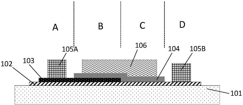
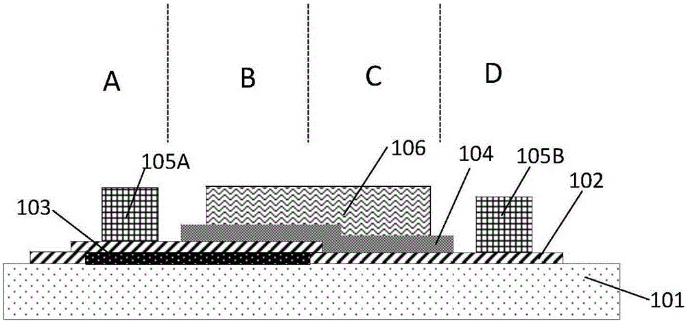
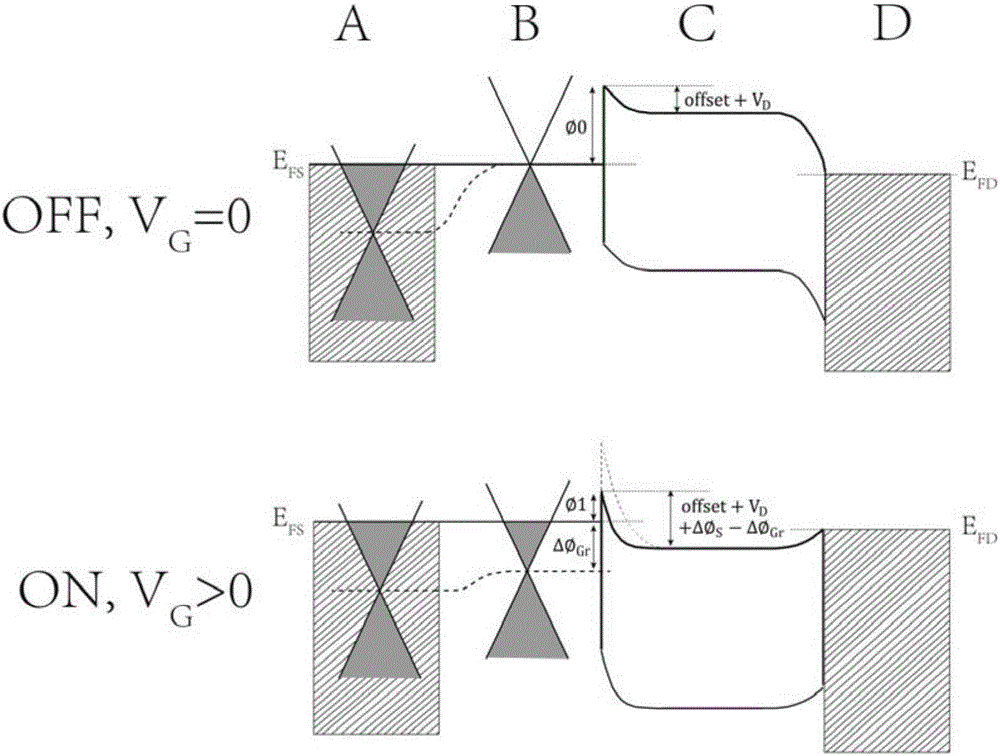
[0035] The heterojunction carbon nanotube field effect transistor of the present invention, such as Figure 1A and Figure 1B As shown, it includes: insulating substrate 101, carbon nanotube 102, graphene layer 103, gate dielectric layer 104, source (drain) electrode 105, gate electrode 106, wherein: described graphene 103 and carbon nanotube 102 constitute The heterojunction channel, the graphene 103 and the carbon nanotube 102 overlap, and the graphene 103 is on the carbon nanotube 102 as Figure 1A The first structure of the graphene 103 under the carbon nanotube 102 is Figure 1A The first structure; the gate structure is composed of a gate dielectric 104 and a gate electrode 10...


PUM

PropertyMeasurementUnit
thicknessaaaaaaaaaa

Abstract

The invention provides a heterojunction carbon nano-tube field effect transistor of which a subthreshold swing is smaller than 60 millivolt/magnitude in the room temperature and a preparation method thereof. The device uses the semiconductor carbon nano-tube as the active layer, the heterojunction formed by the graphene layer and the semiconductor carbon nano-tube is used as the source end of the device, the gate medium and the gate electrode modulate the carbon nano-tube channel and the graphene/carbon nano-tube junction at the same time, so that the turn-off of the transistor is accelerated by using the character that the graphene/carbon nano-tube junction barrier is modulated by the gate voltage. The transistor can control the polarity through the selection of the source-drain metal, namely the metal of high power function is used as the source-drain electrode for realizing the p-type field effect transistor, and the metal of low power function is used as the source-drain electrode for realizing the n-type field effect transistor.

Description

technical field [0001] The invention belongs to the field of solid electronic transistor devices, and in particular relates to a nanometer heterojunction field effect transistor and a preparation method thereof. Background technique [0002] The metal‐oxide‐semiconductor (MOS) field‐effect‐transistor (FET) is the basis for building modern integrated circuits. Field-effect transistors are switched by gate voltage, and their turn-off speed is described by sub-threshold swing. The smaller the sub-threshold swing, the faster the turn-off speed of the transistor. For conventional MOSFET devices, the sub-threshold swing is limited by the thermally excited carrier concentration, and the limit value at room temperature is 60 mV / order. In general, due to insufficient gate efficiency and parasitic effects, sub-threshold The threshold swing will be greater than 60 mV / order. The sub-threshold swing of 60mV / Dec limits the reduction of the threshold voltage of the field effect transisto...

Claims


Application Information

Patent Timeline
Patent Type & Authority Applications(China)
IPC IPC(8): H01L29/78H01L21/336H01L29/10H01L29/06
CPCH01L29/0684H01L29/1033H01L29/66477H01L29/78
Inventor 邱晨光徐琳张志勇彭练矛
Owner BEIJING HUA TAN YUAN XIN ELECTRONICS TECH CO LTD
Why Eureka
Try Eureka