Fin part and finned-type field-effect transistor and forming method thereof

A technology of fins and sub-fins, applied in the field of semiconductor manufacturing, can solve the problems of poor performance of fin-type field effect transistors, slow charge diffusion, threshold voltage shift, etc., achieve uniform morphology, improve migration rate, increase effect of stress

Active Publication Date: 2014-02-12
SEMICON MFG INT (SHANGHAI) CORP
View PDF4 Cites 23 Cited by
  • Summary
  • Abstract
  • Description
  • Claims
  • Application Information

AI Technical Summary

Problems solved by technology

[0006] In the fin field effect transistor formed in the prior art, the fin 11 is perpendicular to the surface of the substrate 10, which has no stress effect on the channel region, the charge diffusion speed in the channel region is relatively slow, and the performance of the fin field effect transistor is poor
Moreover, the uniformity of the topography of the sidewalls of the fins 11 formed in the prior art is relatively poor, and the difference in the topography of the sidewalls of the fins 11 will cause the threshold voltage of the fin field effect transistor to shift, affecting FinFET Stability

Method used


Image

  • Fin part and finned-type field-effect transistor and forming method thereof
  • Fin part and finned-type field-effect transistor and forming method thereof
  • Fin part and finned-type field-effect transistor and forming method thereof

Examples


Embodiment Construction

[0025] In order to make the above-mentioned objects, features and advantages of the present invention more obvious and understandable, the specific embodiments of the present invention will be described in detail below with reference to the accompanying drawings.

[0026] In the following description, many specific details are set forth in order to fully understand the present invention, but the present invention can also be implemented in other ways different from those described here, so the present invention is not limited by the specific embodiments disclosed below.

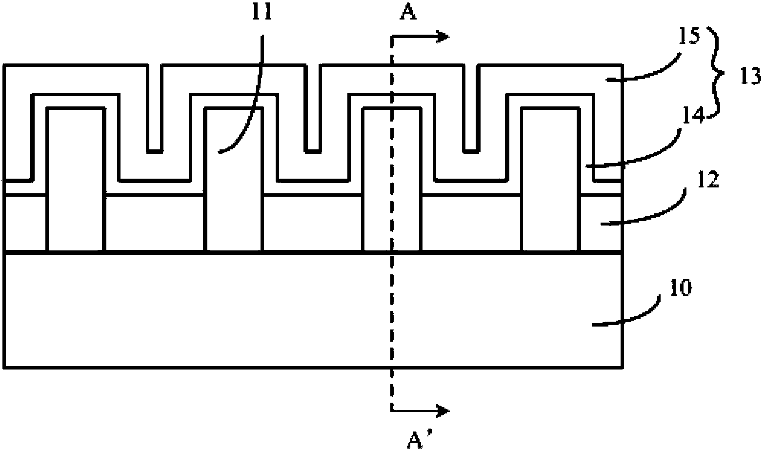
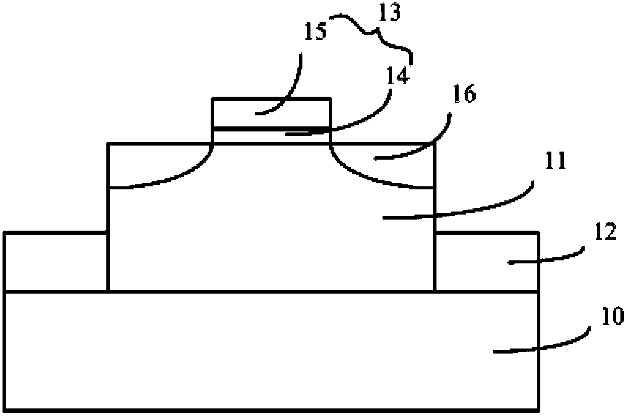
[0027] As mentioned in the background art section, the fins of the fin-type FETs formed in the prior art are perpendicular to the substrate, and the fins have no stress on the channel region of the fin-type FETs including the fins, and the charges in the channel region The diffusion speed is slow, and the performance of the fin-type FET is poor. In addition, the conventionally formed sidewalls of the fin have poor...


PUM


Abstract

The invention discloses a fin part and a finned-type field-effect transistor and a forming method of the fin part and the finned-type field-effect transistor. The forming method of the fin part includes the steps that a substrate is provided; mask layers provided with multiple first openings are formed on the surface of the substrate, and the first openings are exposed out of the substrate; the substrate is etched with the mask layers provided with the first openings as a mask, so that multiple grooves are formed; insulation layers are filled into the grooves; the mask layers are etched back along the first openings, the width of the first openings is increased, and multiple second openings are formed in the mask layers; insulation layers are etched along the second openings with the mask layers as a mask so that the insulation layers can remain with a preset certain thickness, and the substrate among the remaining insulation layers with the preset thickness serves as first auxiliary fin parts; the substrate above the first auxiliary fin parts is etched to form second auxiliary fin parts located on the first auxiliary fin parts and third auxiliary fin parts located on the second auxiliary fin parts. According to the fin part and the finned-type field-effect transistor and the forming method of the fin part and the finned-type field-effect transistor, stability of the finned-type field-effect transistor is improved.

Description

Technical field [0001] The invention relates to the technical field of semiconductor manufacturing, in particular to a fin, a fin field effect tube, and a method for forming the fin and fin field effect tube. Background technique [0002] With the rapid development of semiconductor manufacturing technology, semiconductor devices are moving towards higher component density and higher integration. As the most basic semiconductor device, transistors are currently being widely used. Therefore, as the element density and integration of semiconductor devices increase, the gate size of transistors is becoming shorter and shorter. However, the shorter the gate size of the transistor will cause the transistor to produce a short channel effect, which in turn will generate leakage current, and ultimately affect the electrical performance of the semiconductor device. [0003] In order to overcome the short channel effect of the transistor and suppress the leakage current, the prior art propos...

Claims


Application Information

Patent Timeline
Patent Type & Authority Applications(China)
IPC IPC(8): H01L21/336H01L29/78H01L29/06
CPCH01L29/0603H01L29/0657H01L29/66068H01L29/66795H01L29/7842H01L29/785
Inventor 王新鹏三重野文健张海洋
Owner SEMICON MFG INT (SHANGHAI) CORP
Why Eureka
Try Eureka