Deep trench filling method

A filling method, deep trench technology, applied in electrical components, semiconductor/solid-state device manufacturing, circuits, etc., can solve problems such as increased pattern density, inability to play a protective role, and inability to form good coverage of filling materials, to prevent defects , strengthen protection, improve the effect of electrical performance

Active Publication Date: 2014-02-12
SHANGHAI HUAHONG GRACE SEMICON MFG CORP
View PDF2 Cites 9 Cited by
  • Summary
  • Abstract
  • Description
  • Claims
  • Application Information

AI Technical Summary

Problems solved by technology

[0007] However, when the size of the groove pattern becomes larger (such as the width of the groove>0.8um), or when the density of the pattern increases (such as>2%), or when the depth of the groove is very deep (such as>2um), the filling material cannot be formed well. Coverage, which is very thin at the top of the trench, especially at the corners, and therefore does not provide protection during the subsequent shallow trench etch

Method used


Image

  • Deep trench filling method
  • Deep trench filling method
  • Deep trench filling method

Examples


Embodiment Construction

[0044] like Figure 4 As shown, it is a flow chart of the deep trench filling method of the embodiment of the present invention; the deep trench filling method of the embodiment of the present invention includes the following steps:

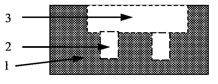
[0045] Step 1, using a photolithographic etching process to form a deep groove on the substrate, the critical dimension of the deep groove is that the width of the deep groove is greater than 0.8 microns, the depth of the deep groove is greater than 2 microns, and the depth The trench aspect ratio is greater than 3, and the pattern density of the deep trench is greater than 2%.

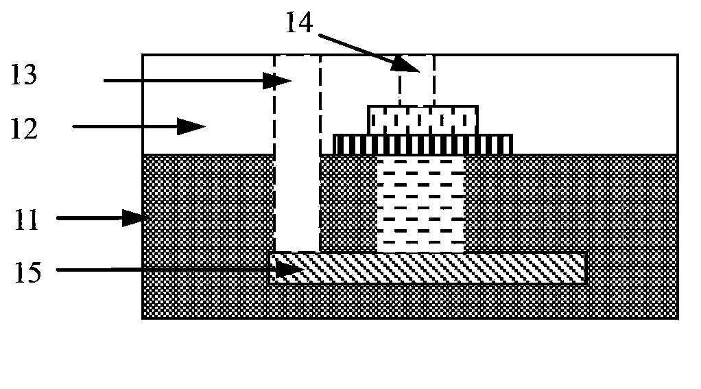
[0046] The substrate is a silicon chip; or the substrate is a silicon chip plus an insulating film formed on the silicon chip; or the substrate is a silicon dioxide layer. by Figure 1B The second example in which grooves of different depths are formed on the same substrate is taken as an example. The substrate is a silicon substrate 11 plus an insulating film 12 forme...


PUM

PropertyMeasurementUnit
depthaaaaaaaaaa
thicknessaaaaaaaaaa
thicknessaaaaaaaaaa

Abstract

The invention discloses a deep trench filling method which comprises the steps of forming a deep trench in a substrate, carrying out surface pretreatment on the surface of the substrate, heating the substrate, spouting pure water on the surface of the substrate to carry out pre-infiltration, forming a first photoresist layer on the surface of the substrate and carrying out heat reflux on the first photoresist layer. The process of photoresist heat reflux is added after the surface of the substrate is gelatinized and before the photoresist is softly baked. As the photoresist has much solvent during heat reflux, the photoresist has good liquidity. The photoresist is enabled to generate reflux through heating, thereby increasing the thickness of the photoresist in the top corner of the deep trench and strengthening the protection of the top corner of the trench. The deep trench can be protected in the process of etching trenches of different depths through two times of photo etching, defects can be prevented from being formed in the top of the deep trench, and the electric property of devices can be improved.

Description

technical field [0001] The invention relates to a semiconductor integrated circuit manufacturing process method, in particular to a deep trench filling method. Background technique [0002] In semiconductor manufacturing, it is often necessary to form trenches of different depths in the same substrate, and often the depths are quite different. like Figure 1A Shown is a schematic diagram of the first example of trenches with different depths formed on the same substrate in the prior art; the first example is an example of using copper interconnects in a typical logic device and using a double damascene structure In the first example, a deep trench 2 and a shallow trench 3 are formed on the SiO2 substrate 1, wherein the deep trench 2 is used as a contact hole, and the shallow trench 3 is used as an interconnection metal of the contact hole. [0003] like Figure 1B Shown is a schematic diagram of a second example of trenches with different depths formed on the same substrat...

Claims


Application Information

Patent Timeline
Patent Type & Authority Applications(China)
IPC IPC(8): H01L21/762
CPCH01L21/31058H01L21/76814H01L21/76819
Inventor 王雷李伟峰
Owner SHANGHAI HUAHONG GRACE SEMICON MFG CORP
Why Eureka
Try Eureka