

Complementary field effect transistor with double-work function metal gates and manufacturing method thereof
A complementary field effect and dual work function technology, which is applied in transistors, semiconductor/solid-state device manufacturing, semiconductor devices, etc., can solve problems such as the difficulty in manufacturing metal gates with double-band edge work functions
- Summary
- Abstract
- Description
- Claims
- Application Information
AI Technical Summary
Problems solved by technology
Method used
Image

Examples
Embodiment Construction
[0024] Embodiments of the present invention will be described below with reference to the drawings. Elements and features described in one drawing or one embodiment of the present invention may be combined with elements and features shown in one or more other drawings or embodiments. It should be noted that representation and description of components and processes that are not related to the present invention and known to those of ordinary skill in the art are omitted from the drawings and descriptions for the purpose of clarity.
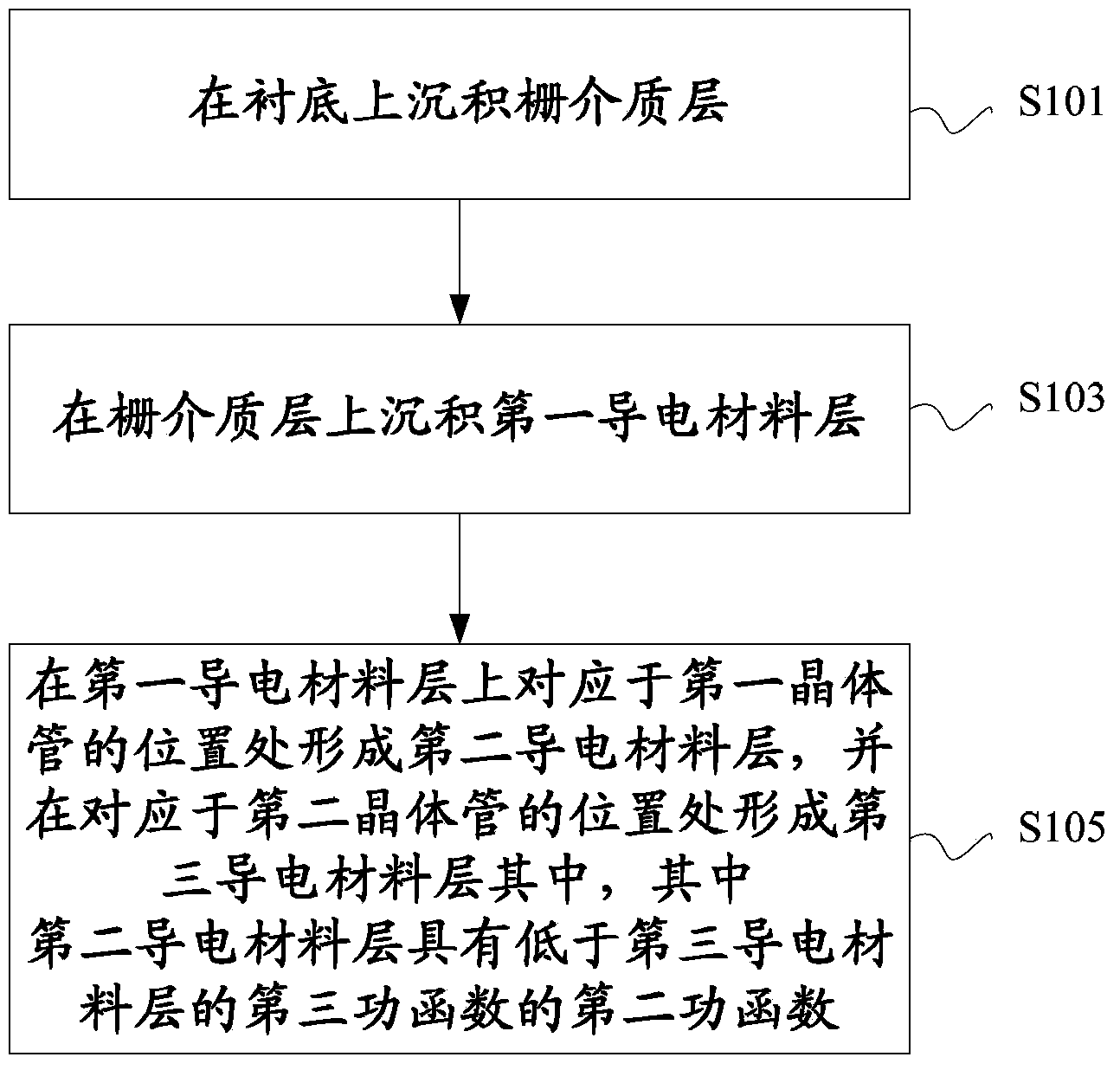
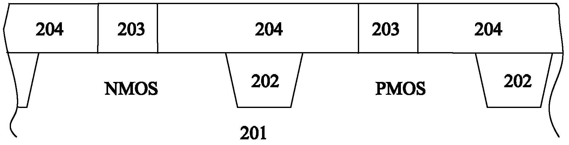
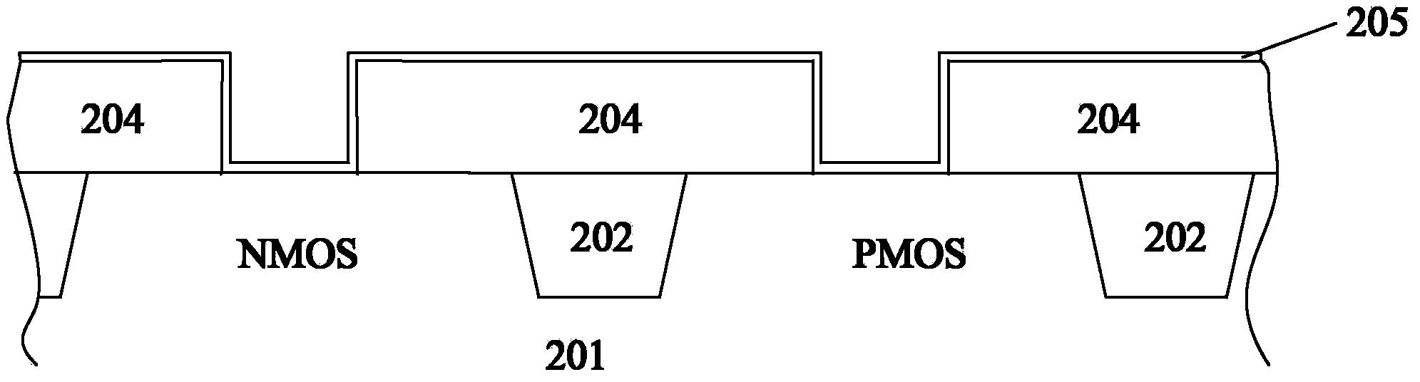
[0025] A complementary field effect transistor (CMOS) with a dual work function metal gate and a manufacturing method thereof are described below according to an embodiment of the present invention. Transistors used in the formation of semiconductor devices are classified as NMOS or PMOS according to the type of main carriers migrating through their channel regions. Electrons are the main carriers in NMOS transistors, while holes are the main carr...
PUM
 Abstract
Description
Claims
Application Information