Method for utilizing photo-crosslinking polymers to conduct thin film packaging on organic electronic device

A technology of organic electronic devices and thin film packaging, applied in the fields of electric solid devices, electrical components, photovoltaic power generation, etc., can solve problems such as increased cost, time consumption limitation, and little research on packaging layers.

Inactive Publication Date: 2014-02-12
JILIN UNIV
View PDF2 Cites 7 Cited by
  • Summary
  • Abstract
  • Description
  • Claims
  • Application Information

AI Technical Summary

Problems solved by technology

Although these encapsulation films have met the industrial requirements for a lifetime of more than 10,000 hours, there are still 2 unresolved issues with this deposition method for fabricating inorganic structures: first, their encapsulation process should be carried out in an environment suitable for organic electronic devices , usually, the low-temperature process of high-quality inorganic layer needs to use plasma enhancement, or very slow deposition technology (such as atomic layer deposition), but the above-mentioned technology will increase the cost and consume time, which seriously limits the scale of industrial production of organic electronic products
However, little research has been done on solution-processed encapsulation layers

Method used


Image

  • Method for utilizing photo-crosslinking polymers to conduct thin film packaging on organic electronic device
  • Method for utilizing photo-crosslinking polymers to conduct thin film packaging on organic electronic device
  • Method for utilizing photo-crosslinking polymers to conduct thin film packaging on organic electronic device

Examples


Embodiment 1

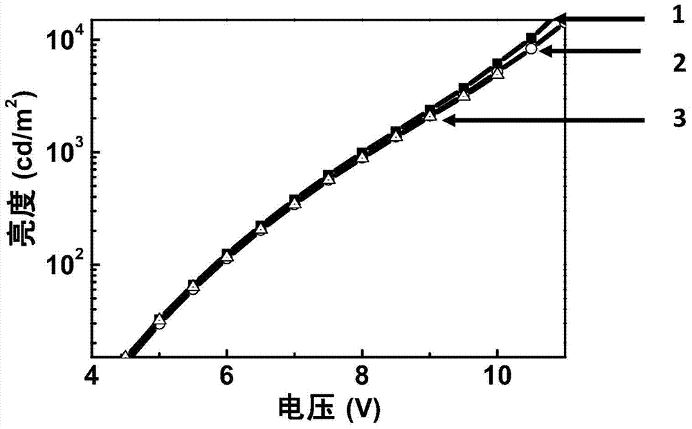
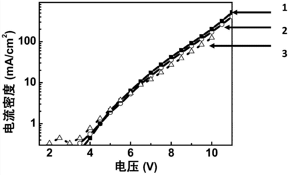
[0028] We prepared the structure as: glass / ITO / MoO 2 (5nm) / mMTDATA (30nm) / NPB(20nm) / Alq(50nm) / LiF(1nm) / Al OLED device. On this basis, A, B, and C three groups of devices were prepared. Among them, the devices in group A are not packaged, the devices in group B are packaged with glass cover (GCE), and the devices in group C are packaged in 16 μm NOA63.

[0029] The preparation process is as follows:

[0030] [1] The substrate material is ITO glass. First, the ITO glass is repeatedly scrubbed and cleaned with acetone and ethanol cotton balls;

[0031] [2] Put the scrubbed substrate into a clean beaker, then ultrasonically use acetone, ethanol, and deionized water for 10 minutes each, and then dry it in an oven to obtain a clean substrate free of chemical impurities and fine particles on the surface. end;

[0032] [3] Place the processed substrate in a multi-source organic molecular vapor deposition system, the vacuum of the system can reach 10 -5 Pa, the vacuum degree of th...

Embodiment 2

[0035] Example 2: Electrical testing of equivalent Ca thin films of organic electronic devices

[0036] In order to accurately evaluate the barrier performance of the packaging film we prepared to water vapor, we have prepared the equivalent Ca thin film electrical test device of the organic electronic device that is spin-coated with NOA63 packaging film described in Example 1, and its device structure and parameters are : Ca(200nm) / Al(100nm) / NOA63(16μm);

[0037] Ca thin film electrical test device structure such as Figure 4 As shown, a glass substrate 41, a simple Ca film 42, two discrete Al contact electrodes 43, and a photocrosslinked polymer packaging film layer 44 are composed;

[0038] Ca elemental film (length 10mm, width 10mm, thickness 200nm) was prepared in the middle of the glass substrate (length 25mm, width 25mm), and the two discrete Al contact electrodes were convex structures (the length of the large area was 24mm, the largest The width of the area is 4mm, ...


PUM

PropertyMeasurementUnit
Thicknessaaaaaaaaaa
Thicknessaaaaaaaaaa
Resistivityaaaaaaaaaa

Abstract

The invention provides a method for utilizing photo-crosslinking polymers to conduct thin film packaging on an organic electronic device, and belongs to the technical field of organic electronic devices. According to the method for utilizing the photo-crosslinking polymers to conduct thin film packaging on the organic electronic device, permeation of water vapor and oxygen into the organic electronic device can be effectively obstructed. Thin films formed through the method have stable chemical and physical properties, and the thin films are suitable for the flexible organic electronic device due to the potential material property of the thin films. The method includes the steps that the organic electronic device with an anode, a functional layer and a metallic cathode structure is manufactured on a substrate; then, the photo-crosslinking polymers are dripped to a metallic cathode of the organic electronic device in a hanging mode, and an organic packaging thin film is acquired through a spin coating method; eventually the organic electronic device coated with the organic packaging thin film is cured under the ultraviolet condition, and then the organic electronic device is packaged.

Description

technical field [0001] The invention belongs to the technical field of organic electronic devices, and in particular relates to a method for encapsulating organic electronic devices with a thin film by using a photocrosslinked polymer. The encapsulation method can effectively block the penetration of water vapor and oxygen into the organic electronic devices. The film formed by this method has stable chemical and physical properties, and its material properties are more potentially suitable for flexible organic electronic devices. Background of the invention [0002] Organic electronic devices have the characteristics of wide sources of materials, rich colors and the ability to form flexible devices. However, there are still many problems in the industrialization of organic electronic devices. One of the key problems is that organic devices are sensitive to water and oxygen in the air, which leads to a decrease in their lifespan. Therefore, organic electronic devices must b...

Claims


Application Information

Patent Timeline
IPC IPC(8): H01L51/40H01L51/48H01L51/56
CPCY02E10/549H10K50/844
Inventor 段羽杨丹陈平王潇杨永强
Owner JILIN UNIV
Why Eureka
Try Eureka