Flexible organic thin film transistor and fabrication method thereof

An organic thin film and transistor technology, applied in the field of high mobility flexible organic thin film transistors and their preparation, can solve problems such as difficult preparation methods, and achieve the effects of optimized spin coating process, good flexibility, and low operating voltage

Active Publication Date: 2019-04-16
CENT SOUTH UNIV
View PDF4 Cites 6 Cited by
  • Summary
  • Abstract
  • Description
  • Claims
  • Application Information

AI Technical Summary

Problems solved by technology

Using a simple and easy-to-operate solution-based fabrication process, organic thin-film transistors on rigid substrates can provide 2 /Vs device mobility, but on flexible substrates, the mobility of organic thin film transistors is difficult to break through 10cm 2 /Vs, the inventor analyzes that its reason is: on the one hand, it is more difficult to deposit a high-q

Method used


Image

  • Flexible organic thin film transistor and fabrication method thereof
  • Flexible organic thin film transistor and fabrication method thereof
  • Flexible organic thin film transistor and fabrication method thereof

Examples


Embodiment 1

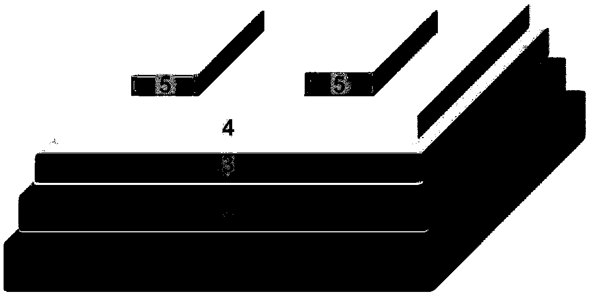
[0043] In this embodiment, the device structure of the flexible organic thin film transistor is as follows figure 1 As shown, it mainly includes a substrate 1 , a gate electrode 2 , an insulating layer 3 , a semiconductor layer 4 and a source-drain electrode 5 . The gate electrode 2 is located on the upper surface of the substrate 1 , the insulating layer 3 is located on the upper surface of the gate electrode 2 , the semiconductor layer 4 is located on the upper surface of the insulating layer 3 , and the source and drain electrodes 5 are located on the upper surface of the semiconductor layer 4 . Among them, the substrate 1 is polyethylene terephthalate (PET), the gate electrode 2 is a conductive ITO film, the insulating layer 3 is a PVP-HDA cross-linked product, and the semiconductor layer 4 is a C8-BTBT:PS film. Pole 5 is metal gold.

[0044] The preparation method of the flexible organic thin film transistor mainly includes the following steps:

[0045] (1) Stir and dis...

Embodiment 2

[0050] In this embodiment, the basic structure refers to Embodiment 1, the substrate 1 is polyethylene terephthalate (PET), the gate electrode 2 is a conductive Ag NWs film, the insulating layer 3 is a PVP-HDA cross-linked product, and the semiconductor layer 4 is a C8-BTBT:PS thin film, and the source and drain electrodes 5 are metal gold or silver. The preparation method of the flexible organic photodetector mainly includes the following steps:

[0051] Refer to the steps (1), (2), and (3) of Example 1. Ag NWs are dispersed in ethanol solution, and then coated on the substrate PET and then thermally annealed and dried to form a very thin staggered stack of Ag NWs conductive film. The Ag NWs / PET substrate prepared by a similar process can be purchased by self-preparation or through merchants. It should be noted that before depositing the insulating layer PVP-HDA film, the gate electrode film ITO in Example 1 can be treated with ultraviolet ozone for 20 minutes to increase t...

Embodiment 3

[0054] In this embodiment, the basic structure refers to embodiment 1, the substrate 1 is polyethylene terephthalate (PET), the gate electrode 2 is a conductive Ag NWs-PEDOT:PSS film, and the insulating layer 3 is PVP-HDA cross-linked material, the semiconductor layer 4 is a C8-BTBT:PS thin film, and the source and drain electrodes 5 are metal gold or silver.

[0055] The preparation method of the flexible organic thin film transistor mainly includes the following steps:

[0056] (1) Add 5% volume of DMSO in the total mixed solution to PEDOT:PSS, and stir at room temperature for 30 min. The blended solution was scraped and deposited on the Ag NWs / PET substrate, and then annealed in the air at 130 °C for 30 min. After annealing, the substrate was placed in N 2 Or store in an argon glove box.

[0057] (2) Referring to the steps (1), (2) and (3) of Example 1, the device preparation can be completed.

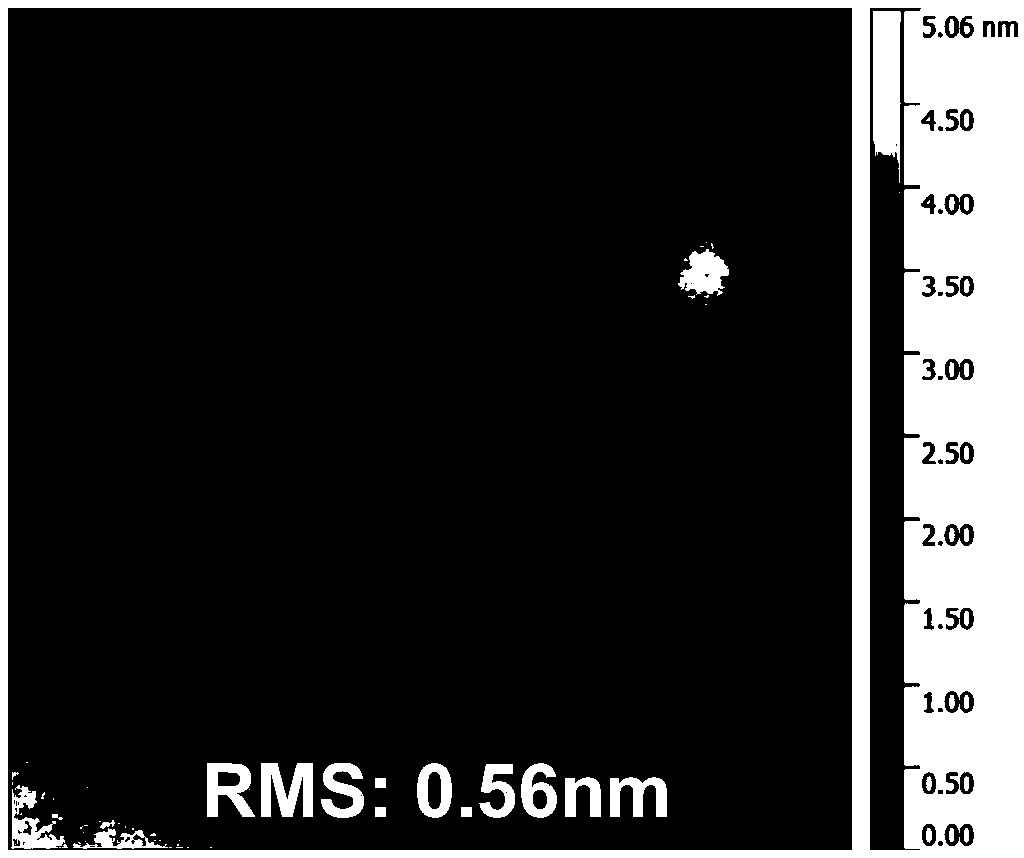
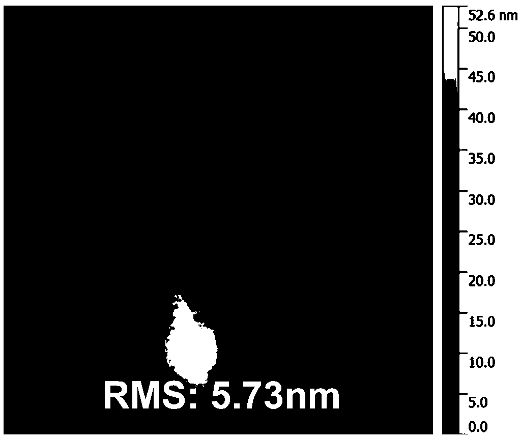
[0058] It has been determined that the flexible organic thin film transistor...


PUM

PropertyMeasurementUnit
Surface roughnessaaaaaaaaaa
Thicknessaaaaaaaaaa

Abstract

The invention discloses a flexible organic thin film transistor and a fabrication method thereof. The flexible organic thin film transistor sequentially comprises a flexible substrate, a gate electrode, an insulation layer, a semiconductor layer and a source-drain electrode, wherein the flexible substrate is polyimide, polyethylene terephthalate, polyethylene naphthalate or paper, the gate electrode is one of an indium tin oxide thin film, aluminum-doped zinc oxide, silver or nanometer silver wire thin film, a conductive polymer PEDOT:PSS or PEDOT:PSS and an AgNWs composite thin film, the insulation layer is a cross-linking agent obtained by esterification reaction of poly4-vinyl-phenol and 4,4'-(hexaisopropenylancetylene) phthalic anhydride, the semiconductor layer is C8-BTBT, and the source-drain electrode is gold, or silver, or nanosilver or PEDOT:PSS. The flexible organic thin film transistor has the advantages of high mobility, low working voltage, ideal switch ratio, favorable flexibility and the like, and a solution method is simple in preparation process and good in economic benefit and can be suitable for production on a large scale.

Description

technical field [0001] The invention belongs to the technical field of semiconductor devices, and in particular relates to a high-mobility flexible organic thin film transistor based on different gate electrodes and a preparation method thereof. Background technique [0002] Organic thin-film transistors have the advantages of simple preparation process, low cost, light weight, wide source of materials, and good flexibility. They are the research focus of next-generation flexible electronic technology and can be widely used in panel displays, sensors, human-machine interfaces, and electronic skins. , wearable devices and other fields. Since the concept of organic thin film transistors was proposed in the 1970s, it has been continuously developed. The substrate has changed from rigid to flexible. More organic materials have been designed and synthesized, which has enriched the choice of materials. The structure of a flexible organic thin film transistor device is generally c...

Claims


Application Information

Patent Timeline
IPC IPC(8): H01L51/05H01L51/00H01L51/30H01L51/40
CPCH10K71/12H10K85/111H10K77/111H10K10/466Y02E10/549Y02P70/50
Inventor 阳军亮刘天娇谢朋杉
Owner CENT SOUTH UNIV
Why Eureka
Try Eureka