Junctionless tunneling field effect transistor and method of forming same

A tunneling field effect, junction-free technology, applied in the manufacture of transistors, semiconductor devices, semiconductor/solid-state devices, etc., can solve the problems of low on-state current of devices, difficult to obtain doping concentration, large subthreshold swing, etc. Achieve the effect of large tunneling current, small process difficulty, and large on-state current

Active Publication Date: 2016-06-01
TSINGHUA UNIV
View PDF5 Cites 0 Cited by
  • Summary
  • Abstract
  • Description
  • Claims
  • Application Information

AI Technical Summary

Problems solved by technology

However, due to the difficulty in obtaining the ideal doping concentration in the existing JLTFET, the actual production of the device still has the problems of low on-state current and large sub-threshold swing.

Method used


Image

  • Junctionless tunneling field effect transistor and method of forming same
  • Junctionless tunneling field effect transistor and method of forming same
  • Junctionless tunneling field effect transistor and method of forming same

Examples


Embodiment Construction

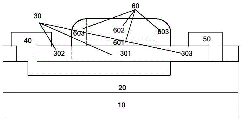
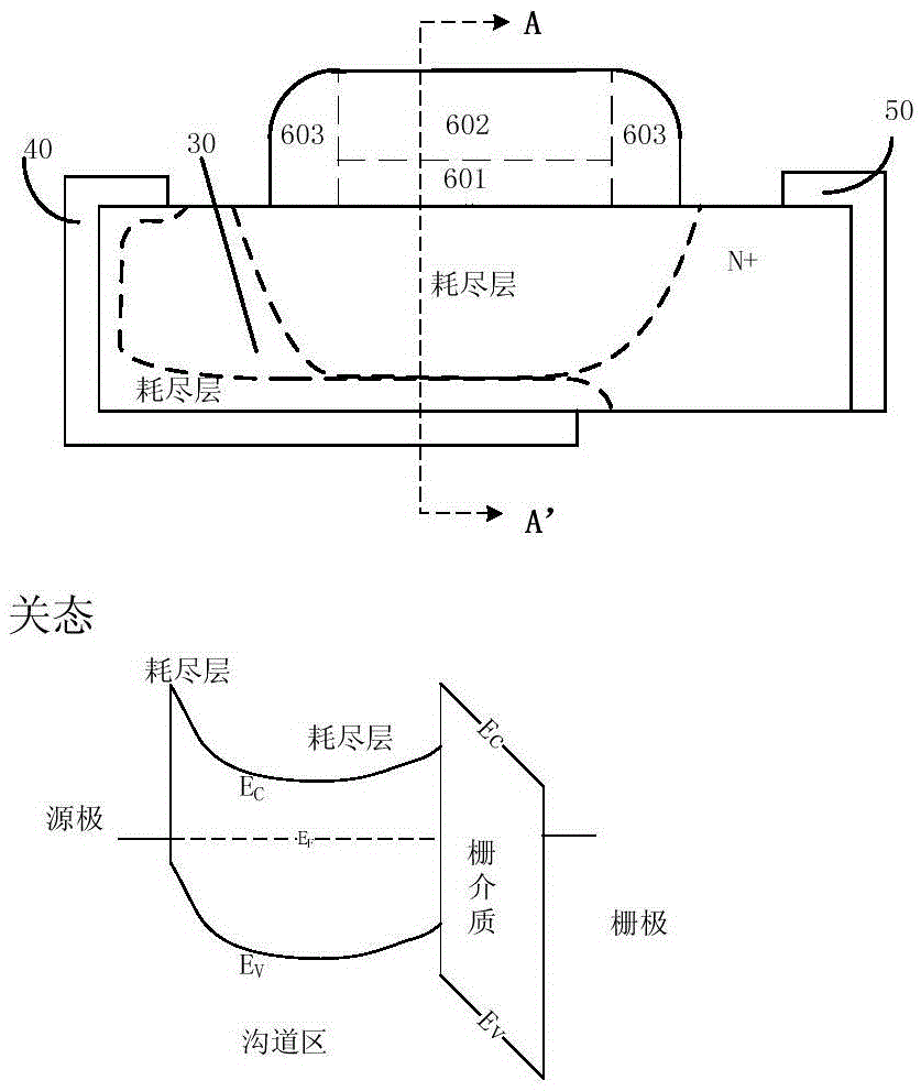
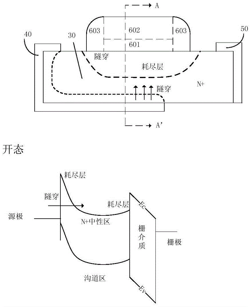
[0030] The embodiments of the present invention are described in detail below. Examples of the embodiments are shown in the accompanying drawings, in which the same or similar reference numerals indicate the same or similar elements or elements with the same or similar functions. The embodiments described below with reference to the accompanying drawings are exemplary, and are intended to explain the present invention, but should not be construed as limiting the present invention.

[0031] In the description of the present invention, it should be understood that the terms "center", "longitudinal", "transverse", "length", "width", "thickness", "upper", "lower", "front", " "Back", "Left", "Right", "Vertical", "Horizontal", "Top", "Bottom", "Inner", "Outer", "Clockwise", "Counterclockwise" and other directions or positions indicated The relationship is based on the orientation or positional relationship shown in the drawings, which is only for the convenience of describing the prese...


PUM


Abstract

The invention provides a junctionless tunneling field effect transistor and a formation method thereof. The junctionless tunneling field effect transistor includes the following components of: a substrate; a liner layer arranged on the substrate; a channel layer which is arranged on the liner layer and includes a channel region arranged in the middle as well as a source region and a drain region arranged at two sides of the channel region, wherein the channel region, the source region and the drain region have the same doping type; a source which coats on the upper surface, a side surface and the lower surface of the source region and coats the lower surface of the channel region, and is in Schottky contact with the channel region; a drain which coats the upper surface and a side surface of the drain region; and a gate stack structure which is located on the channel region. The junctionless tunneling field effect transistor has the advantages of simple structure, large tunneling current, capability of effectively suppressing a short channel effect and the like. The invention also provides a formation method of the junctionless tunneling field effect transistor.

Description

Technical field [0001] The present invention relates to the field of semiconductor technology, in particular to a junctionless tunneling field effect transistor and a method for forming the same. Background technique [0002] Junctionless Tunneling Field Effect Transistor (JLTFET) is widely used because of its small off-state leakage, low subthreshold swing, and effective overcoming the short channel effect. [0003] The channel doping concentration of the existing JLTFET is relatively low doping, and the source region and the drain region have different types of doping concentration, and the source metal is only above or on the side of the source region. The JLTFET has low related state leakage and low subthreshold swing, which effectively overcomes the advantages of short channel effect. However, due to the difficulty in obtaining ideal doping concentration of the existing JLTFET, the actual device still has the problems of low on-state current and large sub-threshold swing. Th...

Claims


Application Information

Patent Timeline
Patent Type & Authority Patents(China)
IPC IPC(8): H01L29/78H01L29/36H01L21/336
CPCH01L29/1029H01L29/66409H01L29/7839
Inventor 刘立滨蒋春生梁仁荣王敬许军
Owner TSINGHUA UNIV
Why Eureka
Try Eureka