
Patsnap Eureka
For R&D, Patsnap Eureka makes reading and utilizing patents & technical documents easy.
Patsnap Eureka AIR
Designed for self-driven R&D workflows. Generate viable solutions, solve complex R&D challenges, empower your innovation with AI.

Patsnap Eureka Materials
Designed for material experts only. Revolutionize your material R&D, from search, analyze, to developing new materials.

TechResearch
Generate reliable direction feasibility study reports for your R&D in just a few steps.

TechSeek
Discover and master advanced knowledge NOW. Basics, ideas, possibilities, all at once.

TechMind
As an expert in R&D Theories, TechMind can generates customized viable solutions instantly.

TechRisk
Analyze your overall solution with one click, know your potential R&D risks in advance.

TechMonitor
Get weekly tech updates, stay abreast of the latest tech innovations and key insights.
Silicon carbide semiconductor device
A semiconductor and silicon carbide technology, applied in the field of silicon carbide semiconductor devices, can solve the problem that JFET is difficult to achieve normally-off characteristics, and achieve the effect of low on-resistance
- Summary
- Abstract
- Description
- Claims
- Application Information
AI Technical Summary
Problems solved by technology
Method used
Image

Examples
Embodiment 1)
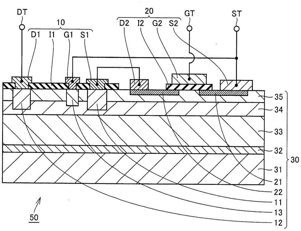
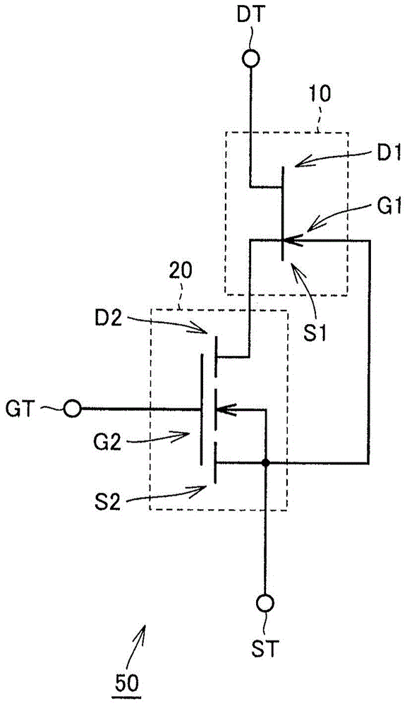
[0035] Such as figure 1 As shown in , the switching element (silicon carbide semiconductor device) 50 in this embodiment has an epitaxial substrate (silicon carbide substrate) 30, a first electrode S1, a second electrode D1, a third electrode G1, a fourth electrode S2, The fifth electrode D2, the sixth electrode G2, the interlayer insulating film I1, and the gate oxide film I2 (gate insulating film).
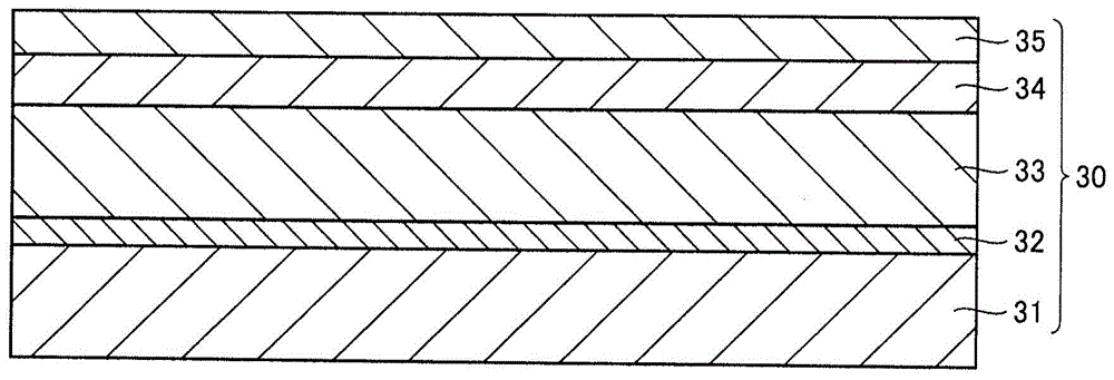
[0036] Epitaxial substrate 30 is made of SiC and has single crystal substrate 31 , buffer layer 32 , n layer (first layer) 34 , upper p layer (second layer) 35 , and lower p layer (third layer) 33 . The n layer 34 has n type (first conductivity type). Each of the lower p layer 33 and the upper p layer 35 has a p type (a second conductivity type different from the first conductivity type). Buffer layer 32 is provided on single crystal substrate 31 . The lower p layer 33 is provided on the buffer layer 32 . The n layer 34 is provided on the lower p layer 33 . An upper p layer...
no. 2 example )
[0058] In this embodiment, the planar layout of the first to sixth electrodes S1 , D1 , G1 , S2 , D2 and G2 will be specifically described.
[0059] exist Figure 7 Floor plan shown in. The first electrode S1 and the fifth electrode D2 are integrated on the epitaxial substrate 30 . Thus, electrical connection can be established between the first electrode S1 and the fifth electrode D2 without particularly providing a wiring structure.
[0060] In addition, the third electrode G1 and the fourth electrode S2 are integrated on the epitaxial substrate 30 . Thus, electrical connection may be established between the third electrode G1 and the fourth electrode S2 without particularly providing a wiring structure.
[0061] It should be noted that, except for the above, the configuration of Embodiment 2 is basically the same as that of Embodiment 1 described above. Therefore, the same or corresponding components will be designated by the same reference numerals, and descriptions th...
no. 3 example )
[0063] Such as Figure 8 As shown in , in the switching element 51 (silicon carbide semiconductor device) in this embodiment, the upper p layer 35 is provided on a part of the n layer 34 , and thus a part of the n layer 34 is exposed. Furthermore, epitaxial substrate 30 has sixth impurity region 14 . The sixth impurity region 14 penetrates the exposed n layer 34 and reaches the lower p layer 33, and has a p-type. Also, the first electrode S1 is electrically connected to the sixth impurity region 14 , and in the present embodiment, the first electrode S1 is in contact with the sixth impurity region 14 . With this configuration, the first electrode S1 and the lower p layer 33 are electrically connected via the p-type sixth impurity region.
[0064] According to the present embodiment, the lower p layer 33 has the same potential as the first electrode S1, and thus the electric field concentration within the n layer 34 can be reduced.
[0065] Note that, except for the above, t...
PUM
 Abstract
Description
Claims
Application Information
 - R&D Engineer
- R&D Manager
- IP Professional
- Industry Leading Data Capabilities
- Powerful AI technology
- Patent DNA Extraction
Browse by: Latest US Patents, China's latest patents, Technical Efficacy Thesaurus, Application Domain, Technology Topic, Popular Technical Reports.
© 2024 PatSnap. All rights reserved.Legal|Privacy policy|Modern Slavery Act Transparency Statement|Sitemap|About US| Contact US: help@patsnap.com