Method for achieving eutectic soldering of chips

A eutectic welding and chip technology, which is used in the manufacture of electrical components, electric solid-state devices, semiconductor/solid-state devices, etc., and can solve the problems of high equipment requirements, long fixture time, and poor applicability.

Active Publication Date: 2014-03-05
THE 41ST INST OF CHINA ELECTRONICS TECH GRP
View PDF5 Cites 14 Cited by
  • Summary
  • Abstract
  • Description
  • Claims
  • Application Information

AI Technical Summary

Problems solved by technology

But the disadvantage of this method is that because the non-compressible area in the chip is very small (generally only 0.05mm border), it is very difficult to mill such a small groove in graphite and make such a small stainless steel pin, and the requirements for equipment It is very high, which increases the difficulty of fixture preparation, and the cost is high; on the other hand, it takes a lon

Method used


Image

  • Method for achieving eutectic soldering of chips
  • Method for achieving eutectic soldering of chips
  • Method for achieving eutectic soldering of chips

Examples


Embodiment 1

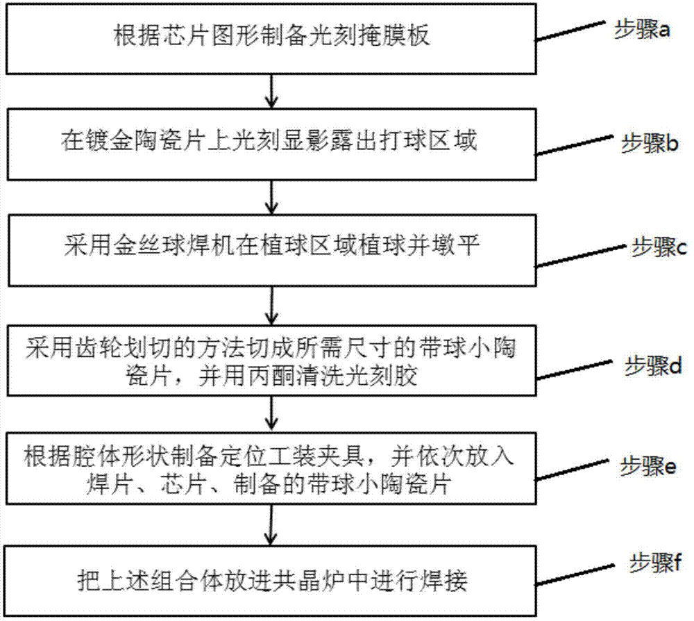
[0031] The purpose of the present invention is to provide a method for providing pressure and positioning for the chip during vacuum eutectic welding of GaAs-based chips, so as to solve the problems that the pressure is not easy to provide and the chip positioning is difficult during vacuum eutectic welding. In order to solve the above problems, the present invention adopts the following technical solutions:

[0032] Step a: Determine the pressable area of ​​the chip according to the pattern of the chip and prepare a photolithographic mask;

[0033] Step b. Remove the conductive glue in the compressible area of ​​the chip on the gold-plated 3 μm ceramic sheet by photolithography and development, and keep the photoresist in the remaining positions;

[0034] Step c, by means of gold wire ball bonding, plant a ball point on the position where the glue is removed on the ceramic sheet as a bump, the height of the bump is higher than the height of the easily collapsed structure such...


PUM

PropertyMeasurementUnit
Diameteraaaaaaaaaa
Heightaaaaaaaaaa

Abstract

The invention provides a method for achieving eutectic soldering of chips. The method comprises the steps of a, compressible areas in the chips are determined, and a photoetching mask panel is manufactured; b, conducting adhesives in the compressible areas of the chips are removed through a photoetching develop method on a gilded ceramic wafer; c, ball points, used as protruding points, are planted at the position, where the adhesives are removed, on the ceramic wafer through a gold ball bonding method; d, the ceramic wafer is cut into small ceramic wafers consistent with the chips in size through a gear cutting method; e, a tool locating clamp is manufactured according to the shapes of cavities to be welded, and a small ceramic wafer pressing block clamp with gold protruding points makes contact with non-circuit areas of the chips through the protruding points; f, a pressing block is arranged on the small ceramic wafer pressing block clamp, and vacuum compressible soldering of the chips is indirectly achieved. The gilded ceramic wafer is used as the base material, the mature photoetching technology and the ball-bonding ball planting technology are used for manufacturing the protruding points to provide effective mechanical support for soldering, and the method is wide in application range.

Description

technical field [0001] The invention belongs to the technical field of chip eutectic welding, and in particular relates to a method for realizing compressive eutectic welding of chips. Background technique [0002] In high-frequency microwave circuits (frequency above 1GHz), the grounding condition of the chip seriously affects the crosstalk and insertion loss of the circuit. At the same time, because the high-power GaAs-based chip has poor thermal conductivity, the connection between the high-power chip and the substrate must have very good microwave grounding capability and good heat dissipation. Vacuum eutectic welding has the advantages of small connection resistance, high heat transfer efficiency, and high heat dissipation intensity, so it is more suitable for welding high-power chips than conductive adhesives. [0003] In order to obtain the eutectic welding effect of high electrical conductivity, high thermal conductivity and low void rate in GaAs-based chips, it is ...

Claims


Application Information

Patent Timeline
IPC IPC(8): H01L21/60
CPCH01L24/83
Inventor 宋志明王斌李红伟吴红莫秀英曹乾涛龙江华
Owner THE 41ST INST OF CHINA ELECTRONICS TECH GRP
Why Eureka
Try Eureka