A three-valued inverter based on CNFETs

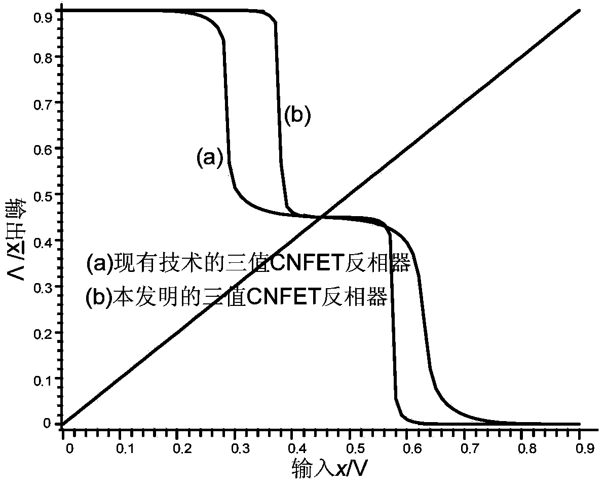
An inverter and base technology, applied in the field of ternary inverters, can solve the problems of voltage fluctuation, large power consumption, and deterioration of the DC characteristic curve.

Active Publication Date: 2014-03-05
NINGBO UNIV
View PDF2 Cites 13 Cited by
  • Summary
  • Abstract
  • Description
  • Claims
  • Application Information

AI Technical Summary

Problems solved by technology

[0004] Literature Lin Sheng, Kim Yong-Bin, Fabrizio Lombardi. A Novel Cntfet-Based Ternary Logic Gate Design[C]. IEEE International Midwest Symposium on Circuits and Systems Conference, 2009: 435-438 (Lin Sheng, Jin Yongbin, Fabrizio Olonbadi. A new type of CNFET-based three-valued logic gate circuit design [C]. Circuits and Systems Midwest International Symposium, 2009: 435-438.) A three-valued CNFET inverter is disclosed, When the input IN is a logic value of 0, the T6 tube is turned on and the output OUT=2; when the IN is a logic value of 2, the T2 tube is turned on, and the output is 0; when the IN is a logic value of 1, the T1, T3, T4, and T5 tubes are turned on , the output is 1, among them, T3 and T4 make their gates and drains connected, which is equivalent to a diode. A resistor with a large resistance value is connected to T5, and between T1 and T3, T4 tubes are symmetrical, so their diode reverse bias resistors are also the same, so that the output value is 1 through voltage division; but because in When a logic value of 1 is input, the T3 and T4 tubes are in the reverse bias state, and the resistance value is large, which will generate a large power consumption. In addition, it can be seen from the DC characteristics of the diode that it is difficult to make the T3 and T4 tubes in a symmetrical state. This will make the output logic value 1, the output terminal OUT with a voltage of 0.45V produce voltage fluctuations, which may not meet the intermediate level we need, and the DC characteristic curve of the inverter will also deteriorate.

Method used


Image

  • A three-valued inverter based on CNFETs
  • A three-valued inverter based on CNFETs
  • A three-valued inverter based on CNFETs

Examples


Embodiment

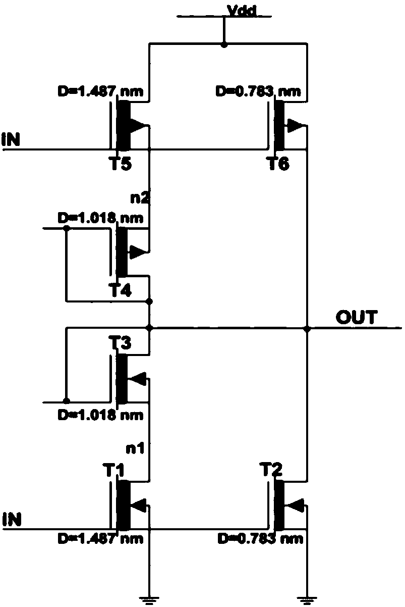
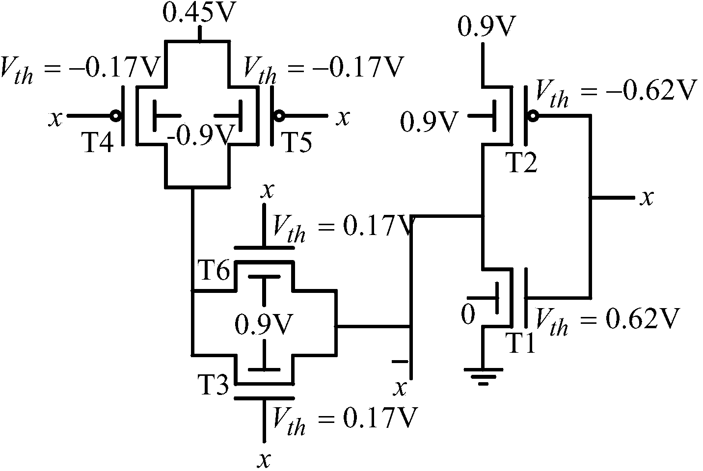
[0013] Example: such as figure 2 As shown, a CNFET-based ternary inverter includes a first CNFET tube T1, a second CNFET tube T2, a third CNFET tube T3, a fourth CNFET tube T4, a fifth CNFET tube T5 and a sixth CNFET tube T6 , the first CNFET tube T1, the third CNFET tube T3 and the sixth CNFET tube T6 are N-type CNFET tubes, the second CNFET tube T2, the fourth CNFET tube T4 and the fifth CNFET tube T5 are P-type CNFET tubes, and the first CNFET tube The threshold voltage of tube T1 is 0.62V, the threshold voltage of the second CNFET tube T2 is -0.62V, the threshold voltage of the third CNFET tube T3 is 0.17V, the threshold voltage of the fourth CNFET tube T4 is 0.17V, and the threshold voltage of the fifth CNFET tube The threshold voltage of T5 is 0.17V, the threshold voltage of the sixth CNFET T6 is -0.17V, the source and base of the first CNFET T1 are grounded, the source of the second CNFET T2, the base of the second CNFET T2 Pole, the base of the third CNFET tube T3 an...


PUM


Abstract

The invention discloses a three-valued inverter based on CNFETs. The three-valued inverter comprises a first CNFET, a second CNFET, a third CNFET, a fourth CNFET, a fifth CNFET, and a sixth CNFET. 0.9V voltage is inputted into the source electrode of the second CNFET, the base electrode of the second CNFET, the base electrode of the third CNFET, and the base electrode of the sixth CNFET. The drain electrode of the third CNFET, the drain electrode of the fourth CNFET, the drain electrode of the fifth CNFET, and the drain electrode of the sixth CNFET are connected. 0.45V voltage is inputted into the source electrode of fourth CNFET and the source electrode of the fifth CNFET. -0.9V voltage is inputted into the base electrode of the fourth CNFET and the base electrode of the fifth CNFET. The grid electrode of the first CNFET, the grid electrode of the second CNFET, the grid electrode of the third CNFET, the grid electrode of the fourth CNFET, the grid electrode of the fifth CNFET, and the grid electrode of the sixth CNFET are connected and a connection point of the same is a signal input end. The drain electrode of the first CNFET, the drain electrode of the second CNFET, the drain electrode of the third CNFET, and the drain electrode of the sixth CNFET are connected and a connection point of the same is a signal output end. The three-valued inverter based on CNFETs has an advantage of low power consumption and satisfies intermediate level needed by users.

Description

technical field [0001] The invention relates to an inverter, in particular to a CNFET-based ternary inverter. Background technique [0002] With the rapid increase of the number of components on the integrated circuit chip, the connection between the internal active device and the external silicon chip has become very complicated, and the wiring area has also continued to increase. The emergence of multi-valued logic provides a new way to solve these problems. Multi-valued logic can increase the single-line transmission information capacity of the circuit, increase the information density of digital circuits, and then reduce the chip area and lead number of integrated circuits. Excessive number of pins has a serious impact on some VLSIs. The application of multi-valued logic can greatly reduce the number of external pins and improve the space and time utilization of the circuit. According to Richards' calculation method, the number of signal values ​​is 3 is the best choice...

Claims


Application Information

Patent Timeline
Patent Type & Authority Applications(China)
IPC IPC(8): H03K19/094
Inventor 汪鹏君唐伟童郑雪松
Owner NINGBO UNIV
Why Eureka
Try Eureka