Dicing tape for processing semiconductor

A semiconductor and dicing technology, which is applied in semiconductor devices, semiconductor/solid device manufacturing, adhesives, etc., can solve the problems of ring frame reuse obstacles, unclear laser marking, low heat resistance, etc., to reduce pollution and prevent The effect of edge collapse and suppression of scatter

Active Publication Date: 2014-03-05
FURUKAWA ELECTRIC CO LTD
View PDF3 Cites 4 Cited by
  • Summary
  • Abstract
  • Description
  • Claims
  • Application Information

AI Technical Summary

Problems solved by technology

However, in this case, if the heat resistance of the base material or the adhesive layer in the tape for semiconductor processing is low, there is a problem that a large amount of adhesive remains on the paste when the package is picked up after the heating process. The part of the package laser mark (package laser mark) that is bonded to the package resin surface (package back side) of the adhesive layer makes the laser mark printed on the package unclear
In addition, there is a problem that when the adhesive tape is peeled off from the ring frame, the adhesive remains on the ring frame, which hinders the reuse of the ring frame which should be reused.

Method used


Image

  • Dicing tape for processing semiconductor
  • Dicing tape for processing semiconductor
  • Dicing tape for processing semiconductor

Examples


Embodiment 1

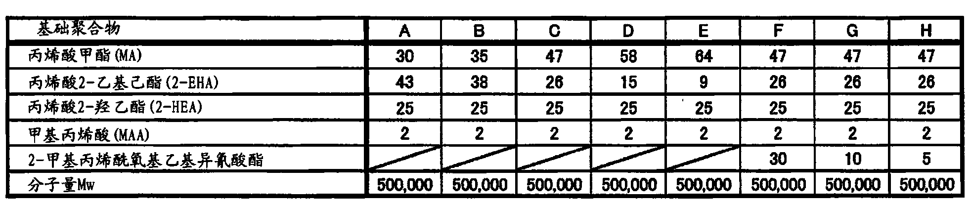
[0068] With respect to 100 parts by mass of the base polymer B, 50 parts by mass of a radiation-curable oligomer obtained by reacting pentaerythritol triacrylate and diisocyanate (the average content of carbon-carbon double bonds per molecule is 6 pieces) was used as a curing method. 2 parts by mass of a polyisocyanate compound (manufactured by Nippon Polyurethane Co., Ltd., trade name CORONATE L) and 3 parts by mass of a photopolymerization initiator (manufactured by Ciba Specialty Chemicals Inc., trade name IRUGACURE651) were mixed to obtain an adhesive combination things.

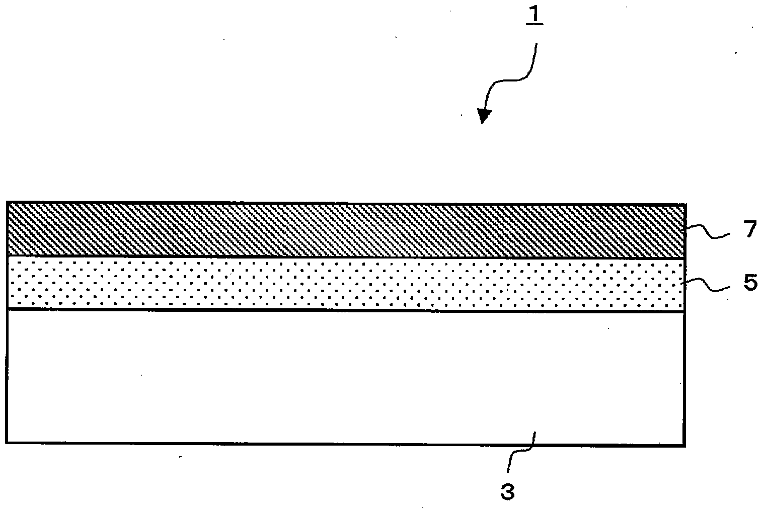
[0069] The obtained adhesive composition was coated on the corona-treated surface of the base film so that the thickness was 20 μm, and a dicing tape for semiconductor processing was produced.

Embodiment 2

[0071] Except having changed the base polymer in an adhesive composition into C, it carried out similarly to Example 1, and obtained the dicing tape for semiconductor processing.

Embodiment 3

[0073] Except having changed the compounding ratio of a radiation-curable oligomer into 25 mass parts, it carried out similarly to Example 2, and obtained the dicing tape for semiconductor processing.


PUM

PropertyMeasurementUnit
thicknessaaaaaaaaaa
glass transition temperatureaaaaaaaaaa
strengthaaaaaaaaaa

Abstract

The purpose of the present invention is to provide a dicing adhesive tape for processing semiconductors, the tape having adhesive strength to sufficiently hold a semiconductor wafer during the process of performing dicing on the wafer, without causing problems such as adhesion to the device or the tray of packages that have been fragmented after the package dicing. The present invention provides a dicing tape for processing semiconductors, characterized in that: a radiation-curing adhesive layer is formed on at least one surface of a substrate film; the adhesive film comprises a resin composition containing, as a base polymer, an acrylic-based polymer; the thickness of the adhesive film is 10 to 30 mum; the adhesive strength of the adhesive layer, after irradiation of an SUS304 with radiation based on JIS Z0237, is 1.0 to 2.0N/25 mm tape width when a 90 DEG peel test is performed; and the peak intensity of a probe tack of the adhesive layer after irradiation with radiation under air atmospheric conditions is 50 to 150 mN/mm2.

Description

technical field [0001] The present invention relates to a dicing tape suitable for fixing and holding a semiconductor wafer when dicing a semiconductor wafer into chips, etc., and particularly relates to a dicing tape for semiconductor processing suitable for high-density packaging semiconductor packaging processing. Background technique [0002] Conventionally, when a semiconductor wafer on which a circuit pattern is formed is separated into chips, a so-called dicing process, a pickup method using a tape for semiconductor processing has been used for fixing the wafer. In this method, a large-diameter wafer is bonded and fixed to a semiconductor processing tape, and is diced into chips. After cleaning and drying, it goes through a pick-up process and is packaged by resin sealing. [0003] In recent years, various companies have developed flip-chip packages having electrodes on the pattern circuit side as one of the methods of miniaturizing semiconductor elements. In this fl...

Claims


Application Information

Patent Timeline
Patent Type & Authority Applications(China)
IPC IPC(8): H01L21/301C09J7/02C09J133/00C09J133/08
CPCC09J133/08C08F2222/1026C09J4/06C09J7/02C09J133/00H01L2221/68381H01L21/6836C08F8/30H01L2221/68336H01L2221/68331H01L2221/68327C08F222/103C09J7/385C09J2203/326C08F220/14C08F220/1808C08F220/06C08F220/20
Inventor 阿久津晃
Owner FURUKAWA ELECTRIC CO LTD
Why Eureka
Try Eureka