Supercharge Your Innovation With Domain-Expert AI Agents!

Method for preventing generation of defects in semiconductor product high temperature rapid annealing

A high-temperature rapid annealing, semiconductor technology, used in semiconductor/solid-state device manufacturing, electrical components, circuits, etc., can solve problems such as product yield decline

Inactive Publication Date: 2014-03-12
SHANGHAI HUAHONG GRACE SEMICON MFG CORP
View PDF3 Cites 0 Cited by
  • Summary
  • Abstract
  • Description
  • Claims
  • Application Information

AI Technical Summary

Problems solved by technology

[0005] The technical problem to be solved by the present invention is to provide a method for preventing defects from occurring during high-temperature rapid annealing of semiconductor products, which can effectively prevent the product yield from declining due to the fact that silicon substrates are prone to react with nitrogen at high temperatures to form defects

Method used


Image

  • Method for preventing generation of defects in semiconductor product high temperature rapid annealing
  • Method for preventing generation of defects in semiconductor product high temperature rapid annealing
  • Method for preventing generation of defects in semiconductor product high temperature rapid annealing

Examples


Embodiment Construction

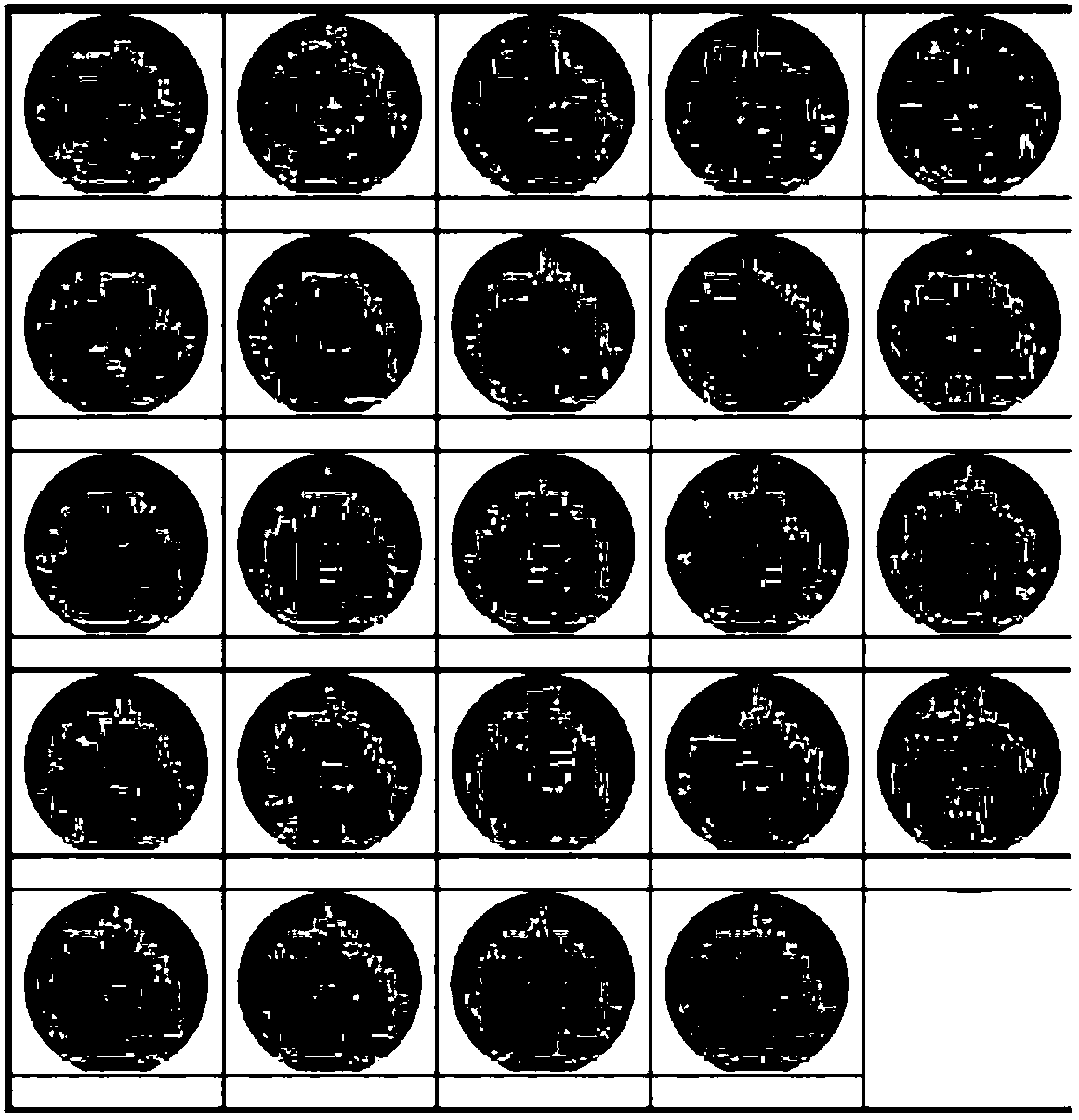
[0014] to combine Figure 5 As shown, when semiconductor products are subjected to high-temperature (greater than 1000°C, duration greater than 10 seconds) rapid annealing after high-dose ion implantation, the silicon surface does not have any protective layer at this time, that is, the silicon surface is exposed. In view of this situation, it is necessary to use argon as the process gas in the heating-up stage, high-temperature continuous stage and cooling-down stage of high-temperature rapid annealing. oxygen to the required level.

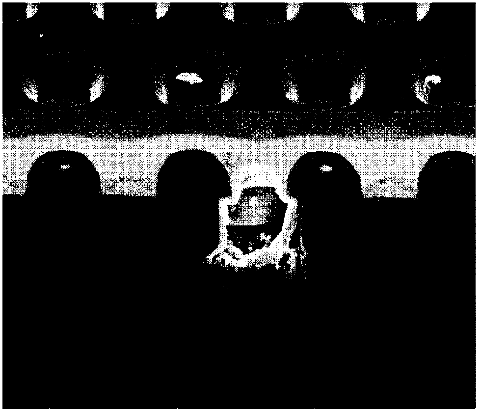
[0015] Off-line experiments show that after high-dose ion implantation and rapid thermal annealing above 1000°C, many porous defects are generated on the surface of the silicon wafer (see Figure 4 ). The mechanism should be that nitrogen and silicon react easily at high temperature to form silicon nitride, and the high tensile stress of silicon nitride will cause cracks, that is, the observed voids. Replace the high-temperature rapid anneali...


PUM


Abstract

The invention discloses a method for preventing generation of defects in semiconductor product high temperature rapid annealing. After an injection with a high dose of being greater than or equal to 1E14ion / cm<2> is performed, a silicon substrate is exposed, wherein argon is adopted to act as technology gas when high temperature annealing is performed; and high temperature refers to temperature which is greater than or equal to 1000 DEG C, and time of duration is greater than or equal to 10 seconds. Decreasing of product yield rate caused by the defects due to the fact that the silicone substrate is liable to react with nitrogen under high temperature can be effectively prevented by the method.

Description

technical field [0001] The invention relates to a manufacturing process method of a semiconductor integrated circuit, in particular to a method for preventing defects from occurring during high-temperature rapid annealing of semiconductor products. Background technique [0002] In the manufacturing process of existing semiconductor products, after the contact hole is cut (the silicon substrate is exposed), in order to reduce the contact resistance, high-dose ion implantation (greater than E15) will be performed. Then, HP8800 equipment will be used for high-temperature (higher than 1000°C) rapid annealing, and TI (titanium) / TIN (titanium nitride) / AL (aluminum) will be used to fill holes after annealing. These products are prone to abnormal leakage. From the results of slicing, it can be confirmed that it is an aluminum nail, that is, the TIN cannot block the AL, causing the AL to penetrate into the silicon substrate and conduct the source and drain of the device (see figure ...

Claims


Application Information

Patent Timeline
Patent Type & Authority Applications(China)
IPC IPC(8): H01L21/324
CPCH01L21/324
Inventor 孙建军端木佳清
Owner SHANGHAI HUAHONG GRACE SEMICON MFG CORP
Features
  • R&D
  • Intellectual Property
  • Life Sciences
  • Materials
  • Tech Scout
  • Unparalleled Data Quality
  • Higher Quality Content
  • 60% Fewer Hallucinations
Learn More