Production method of LED (light emitting diode) chip

An LED chip and manufacturing method technology, which is applied in semiconductor/solid-state device manufacturing, electrical components, circuits, etc., can solve the problems of complex LED chip manufacturing process, smaller ITO effective area, and high product cost, and shorten the chip processing process. , Reduce the cost of chip processing and realize the effect of self-alignment function

Inactive Publication Date: 2014-03-12
FOCUS LIGHTINGS SCI & TECH
View PDF5 Cites 18 Cited by
  • Summary
  • Abstract
  • Description
  • Claims
  • Application Information

AI Technical Summary

Problems solved by technology

[0019] In the prior art, the manufacturing process of LED chips is complicated, and the number of lithography passes is large, and the process repeatedly passes through the same station (such as coating, photolithography, development, deglue, etc.), which is prone to err

Method used


Image

  • Production method of LED (light emitting diode) chip
  • Production method of LED (light emitting diode) chip
  • Production method of LED (light emitting diode) chip

Examples


Embodiment Construction

[0064] In order to enable those skilled in the art to better understand the technical solutions in the present invention, the technical solutions in the embodiments of the present invention will be clearly and completely described below in conjunction with the drawings in the embodiments of the present invention. Obviously, the described The embodiments are only some of the embodiments of the present invention, not all of them. Based on the embodiments of the present invention, all other embodiments obtained by persons of ordinary skill in the art without making creative efforts shall fall within the protection scope of the present invention.

[0065] Furthermore, repeated reference numerals or designations may be used in different embodiments. These repetitions are only for the purpose of simply and clearly describing the present invention, and do not represent any relationship between the different embodiments and / or structures discussed.

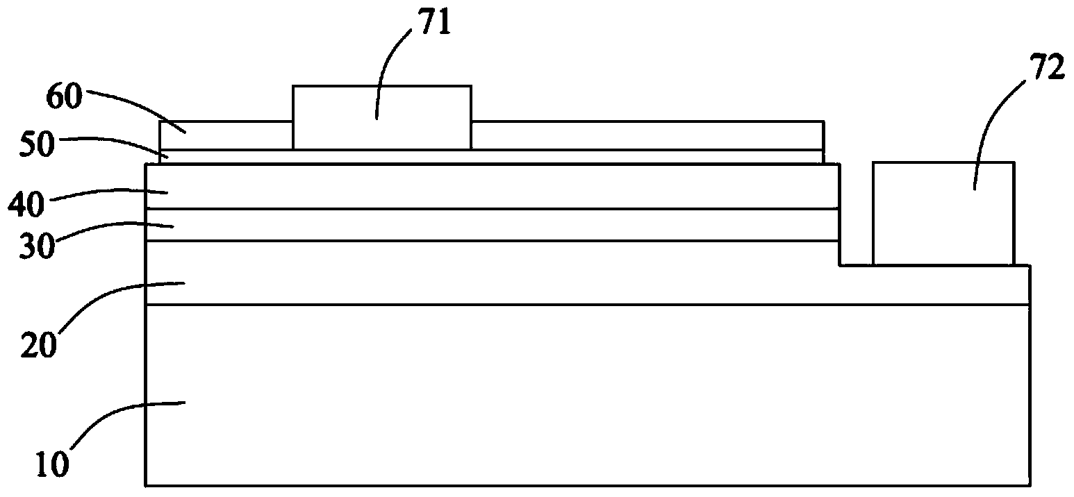
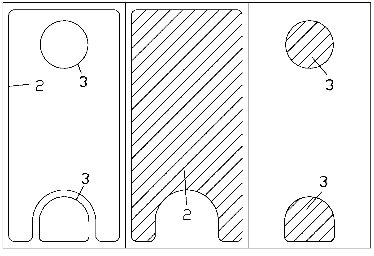
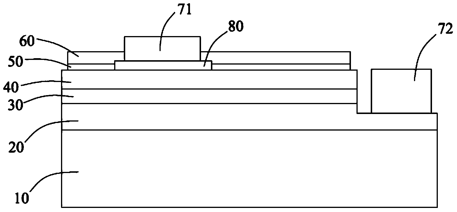
[0066] ginsengfigure 1 Shown is a...


PUM


Abstract

The invention discloses a production method of an LED (light emitting diode) chip. The production method comprises the following steps of providing a substrate, and sequentially producing an N-type semiconductor layer, a luminescent layer and a P-type semiconductor layer on the substrate to form an LED wafer; depositing an ITO (indium oxide) transparent conductive layer on the LED wafer; performing the MESA photoetching on the ITO transparent conductive layer through photoetching glue to form an MESA layer; performing ITO etching on the ITO transparent conductive layer; performing the ICP etching on the LED wafer to form an N-type semiconductor table-board; removing the photoetching glue remained after the MESA photoetching; depositing a passivation layer on the ITO transparent conductive layer and the N-type semiconductor table-board; performing the PAD photoetching on the passivation layer through the photoetching glue to form a PAD layer; performing the passivation etching on the PAD layer, and removing the passivation layer in the area of the PAD layer; producing a P electrode and an N electrode on the etched passivation layer; and removing the photoetching glue remained after the PAD photoetching. By adopting the method, a self-aligning function of the photoetching can be realized, the machining flow of the chip can be shortened, and the machining cost of the chip can be reduced, the ITO light emitting area is increased, and the brightness of the chip is improved.

Description

technical field [0001] The invention relates to the technical field of semiconductor light emitting devices, in particular to a method for manufacturing an LED chip. Background technique [0002] A light-emitting diode (Light-Emitting Diode, LED) is a semiconductor electronic component that can emit light. This electronic component appeared as early as 1962. In the early days, it could only emit red light with low luminosity. Later, other monochromatic light versions were developed. Today, the light that can be emitted has covered visible light, infrared rays and ultraviolet rays, and the luminosity has also increased to a considerable extent. of luminosity. And the use is also used as indicator lights, display panels, etc. from the beginning; with the continuous advancement of technology, light-emitting diodes have been widely used in displays, TV lighting decoration and lighting. [0003] Existing LED chip manufacturing methods usually include five, four or three photoli...

Claims


Application Information

Patent Timeline
IPC IPC(8): H01L33/02H01L33/14H01L21/027
CPCH01L33/0075H01L21/027
Inventor 李忠武魏天使何金霞
Owner FOCUS LIGHTINGS SCI & TECH
Why Eureka
Try Eureka