
Laser device

A laser and grating technology, applied in the field of optical communication, can solve the problems of limited speed and energy consumption, insufficient, and inability to significantly reduce the length of the effective cavity, and achieve the effect of excellent single-mode properties

Inactive Publication Date: 2014-03-12
DANMARKS TEKNISKE UNIV
View PDF3 Cites 5 Cited by
  • Summary
  • Abstract
  • Description
  • Claims
  • Application Information

AI Technical Summary

Problems solved by technology

The shown energy per bit of 357fJ / bit (=12.5mW / 35Gb / s) is unusually small, but insufficient for the above applications
Also the effective cavity length cannot be significantly reduced due to the need for an optical cavity with a certain thickness including the active region for light generation
[0008] Therefore, in currently known solutions, there are limitations on the speed and energy consumption of directly modulating VCSEL structures

Method used


Image

  • Laser device
  • Laser device
  • Laser device

Examples


Embodiment Construction

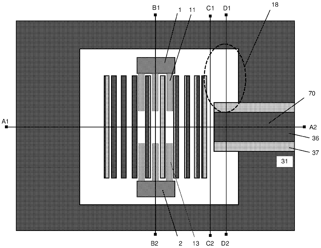
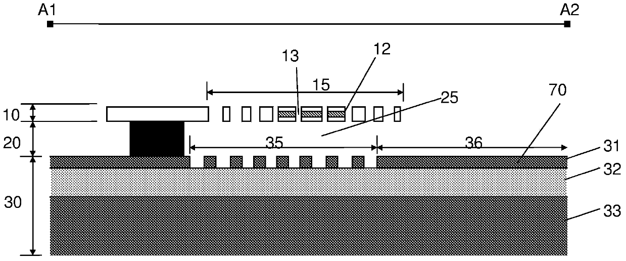
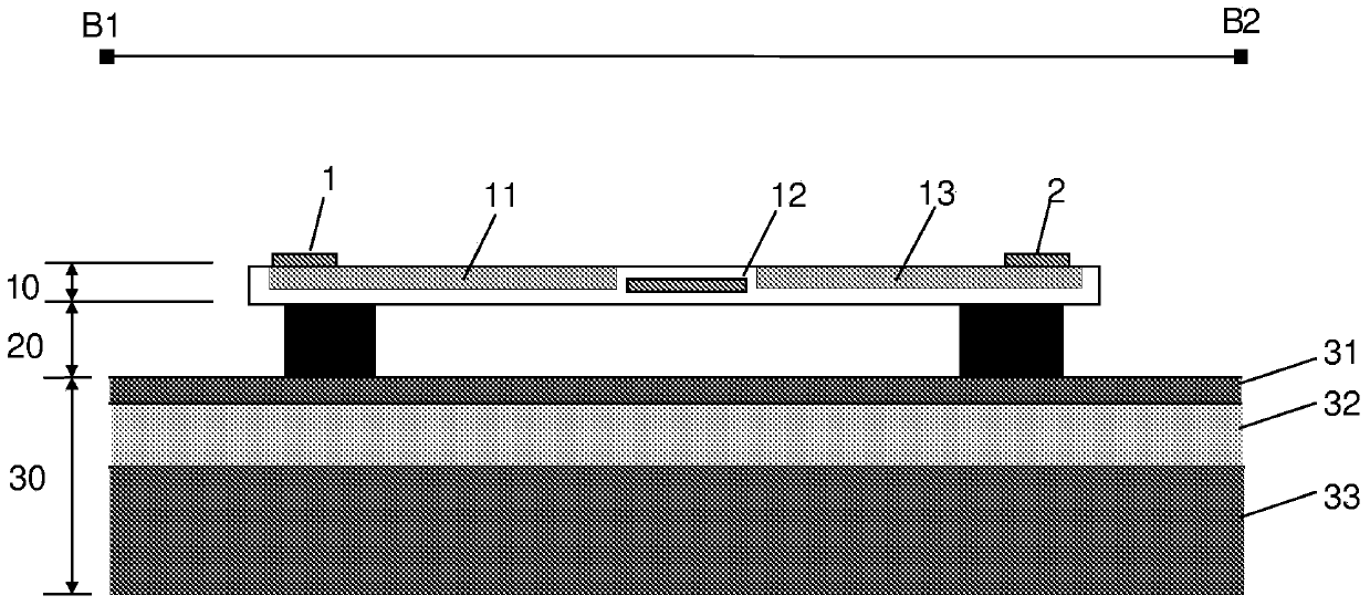
[0078] exist Figures 1A-1E The middle diagram shows an exemplary embodiment of a laser according to the invention. exist Figure 1B is shown along the Figure 1A Cross-sectional device structure of lines A1-A2.

[0079] by first thinking together Figure 1A and 1B , the basic structure of the invention will be best understood. The laser structure includes an active grating region 15 , an air cavity 25 and a passive grating region 35 . An active grating region 15 and a passive grating region 35 are typically placed on each side of the air cavity 25 to form a resonant structure, which forms the laser cavity. Both the active grating 15 and the passive grating 35 may be periodic gratings and act as highly reflective mirrors. The grating 15, 35 is generally periodic in a direction parallel to the plane of the semiconductor structure.

[0080] The periodicity of the active grating 15 can be spatially modulated to focus the reflected light. This results in lateral optical co...


PUM


Abstract

The present invention provides a light source for light circuits on a silicon platform. A vertical laser cavity is formed by a gain region arranged between a first mirror structure and a second mirror structure, both acting as mirrors, by forming a grating region including an active material in a silicon layer in a semiconductor structure or wafer structure. A waveguide for receiving light from the region of the mirrors is formed within or to be connected to the region of the mirrors, and functions as an output coupler for the VCL. Thereby, vertical lasing modes are coupled to lateral in-plane modes of the in-plane waveguide formed in the silicon layer, and light can be provided to e.g. photonic circuits on a SOI or CMOS substrate in the silicon.

Description

technical field [0001] The present invention relates to the field of optical communications, and in particular it relates to high-speed optical communications using semiconductor lasers. Even more particularly, the invention relates to semiconductor lasers suitable for use in or in optical interconnections to silicon chips. The invention also relates to a method of manufacturing a laser and a method of modulating a laser when in use. Background technique [0002] In short-range optical interconnect applications, low energy consumption and high transmission speed of building block devices are becoming key technical issues as data transmission bandwidth increases. Thus, the figure of merit is the energy consumption per transmitted bit. According to the recent technology roadmap provided in [[96]], several 10s fJ / bit are required for optical transmitters for chip-scale optical interconnection in 2015-2020. [0003] As light emitters, vertical-cavity surface-emitting lasers (...

Claims


Application Information

Patent Timeline
Patent Type & Authority Applications(China)
IPC IPC(8): H01S5/026H01S5/02H01S5/183
CPCH01S5/187H01S5/1228H01S5/0424H01S5/1032H01S5/18386H01S5/0425H01S5/021H01S5/026H01S5/0215H01S5/1838H01S5/06226H01S5/1234H01S5/18311H01S5/18319
Inventor 钟日锡
Owner DANMARKS TEKNISKE UNIV
Learn More