Manufacturing method of graphene device

A production method, graphene technology, applied in semiconductor/solid-state device manufacturing, semiconductor devices, electrical components, etc., to achieve the effect of avoiding influence and expanding the scope of application

Active Publication Date: 2014-03-19
SHANGHAI INST OF MICROSYSTEM & INFORMATION TECH CHINESE ACAD OF SCI
View PDF1 Cites 19 Cited by
  • Summary
  • Abstract
  • Description
  • Claims
  • Application Information

AI Technical Summary

Problems solved by technology

However, most of the current research on the preparation process of graphene field effect transistors uses semiconductor silicon as the substrate due to the integration of low-temperature processing technology and high-K dielectric preparation technology. However, on any substrate such as an organic or inorganic substrate, rigidity and Large-scale integration of nanodevices with high performance on flexible substrates remains challenging

Method used


Image

  • Manufacturing method of graphene device
  • Manufacturing method of graphene device
  • Manufacturing method of graphene device

Examples


Embodiment Construction

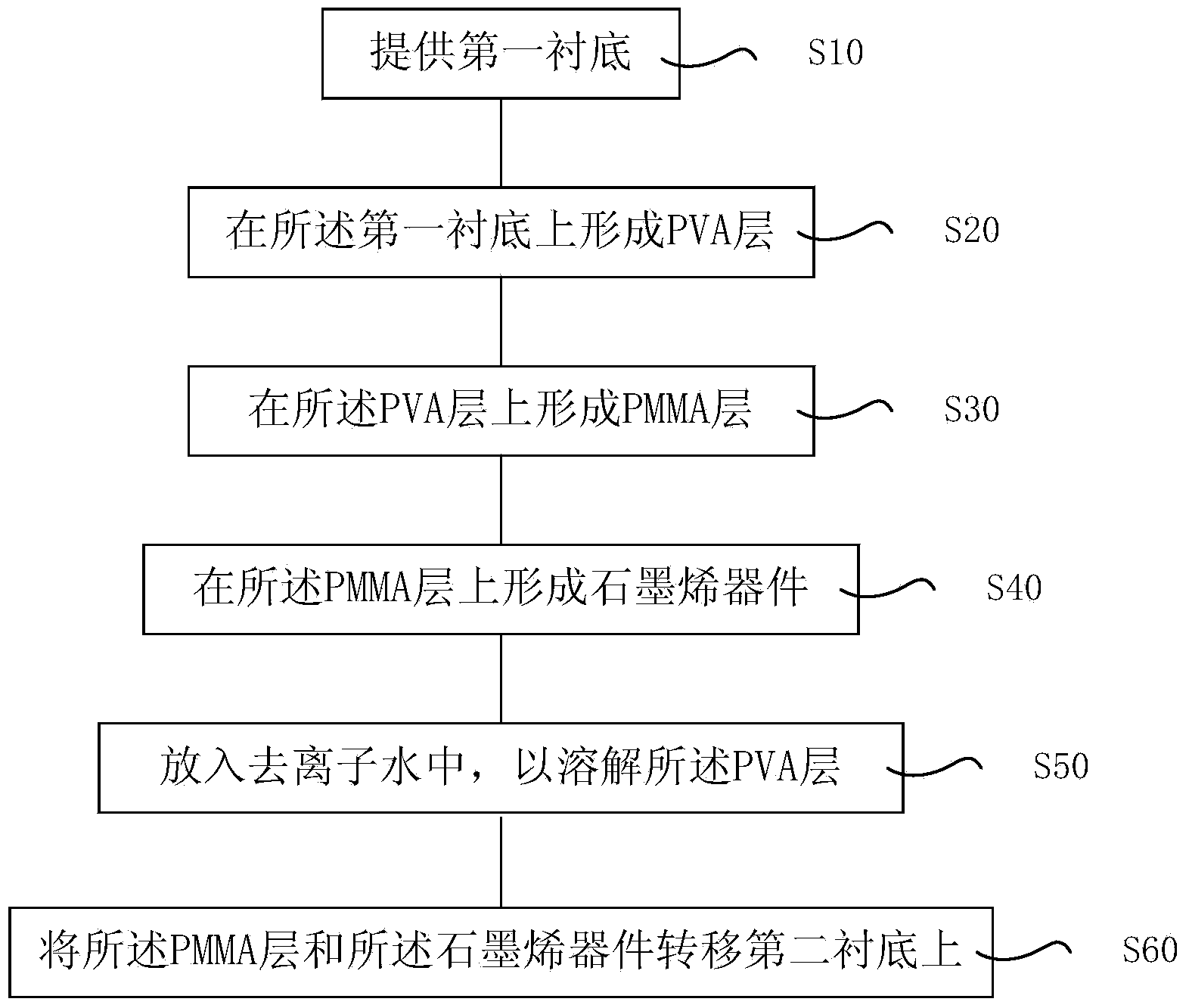
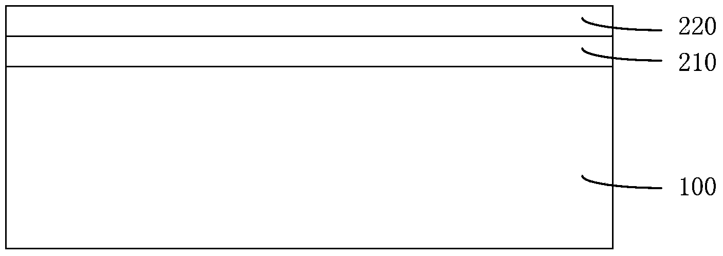
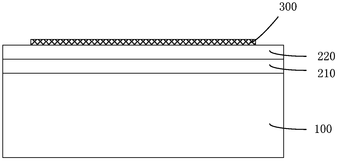
[0039] The present invention will provide a kind of manufacturing process of transferable graphene device, at least comprise: form PVA layer on described first substrate; Form PMMA layer on described PVA layer, prepare graphene on described PMMA layer device, then dissolve the PVA layer, transfer the graphene device and the PMMA layer together to the polyimide substrate, realize the formation of the graphene device on the flexible polymer substrate, and the device switch ratio on the flexible polymer substrate can reach 10 -6 , the device can still work normally after repeated bending.

[0040] In addition, the present invention is also applicable to transferring the prepared graphene device to other substrates, so as to realize the improvement of the function of the graphene electronic device and its wider application.

[0041] Embodiments of the present invention are described below through specific examples, and those skilled in the art can easily understand other advantag...


PUM

PropertyMeasurementUnit
thicknessaaaaaaaaaa
thicknessaaaaaaaaaa
thicknessaaaaaaaaaa

Abstract

The invention provides a manufacturing method of a graphene device. The manufacturing method of the graphene device at least comprises providing a first substrate; forming a PVA (polyvinyl alcohol) layer; forming a PMMA (polymethyl methacrylate) layer on the PVA layer; forming the graphene device on the PMMA layer; putting the first substrate, the PVA layer, the PMMA layer and the graphene device into deionized water to dissolve the PVA layer and to separate the PMMA layer and the graphene device from the first substrate; transferring the PMMA layer and the graphene device to a second substrate. According to the manufacturing method of the graphene device, PMMA serves as the support layer and meanwhile PVA serves as the sacrificial layer; by removing the PVA, the graphene device formed on the PMMA layer and the PMMA layer can be separated from the first substrate simultaneously and then adhered to the second substrate (a polyimide substrate in the embodiment), therefore, the graphene device can be formed on the second substrate. The manufacturing method of the graphene device can widen the application range of the graphene device.

Description

technical field [0001] The invention relates to a semiconductor technology, in particular to a method for manufacturing a graphene device. Background technique [0002] Graphene is a two-dimensional crystal composed of carbon atoms that is stripped from graphite materials. It is only the thickness of one layer of carbon atoms. It is the thinnest and hardest material so far. Its unique structure makes it display a series of peculiar physical properties. Features, such as high electrical conductivity, thermal conductivity, light transmittance, high mobility and mechanical strength, etc. Graphene has a series of important photoelectric properties such as transparency, softness, continuously adjustable energy band structure, and high electron mobility. Graphene-based electronic devices have important application prospects in the field of next-generation nanoelectronic devices, such as light-emitting diodes, Solar cells and nanogenerators, etc. These superior physical propertie...

Claims


Application Information

Patent Timeline
Patent Type & Authority Applications(China)
IPC IPC(8): H01L21/04
CPCH01L21/2007H01L21/7813H01L29/66477
Inventor 王浩敏谢红孙秋娟王慧山吴天如谢晓明江绵恒
Owner SHANGHAI INST OF MICROSYSTEM & INFORMATION TECH CHINESE ACAD OF SCI
Why Eureka
Try Eureka